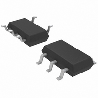
LT6650HS5#TRMPBF Linear Technology, LT6650HS5#TRMPBF Datasheet - Page 9

LT6650HS5#TRMPBF
Manufacturer Part Number
LT6650HS5#TRMPBF
Description
IC REF 400MV R-R BUFFER TSOT23-5
Manufacturer
Linear Technology
Datasheet
1.LT6650CS5TR.pdf
(12 pages)
Specifications of LT6650HS5#TRMPBF
Reference Type
Series
Voltage - Output
400mV
Tolerance
±1.5%
Temperature Coefficient
30ppm/°C
Voltage - Input
1.4 ~ 18 V
Number Of Channels
1
Current - Quiescent
11µA
Current - Output
200µA
Operating Temperature
-40°C ~ 125°C
Mounting Type
Surface Mount
Package / Case
TSOT-23-5, TSOT-5, TSOP-5
Lead Free Status / RoHS Status
Lead free / RoHS Compliant
Current - Cathode
-
Other names
LT6650HS5#PBF
LT6650HS5#PBF
LT6650HS5#PBF
Available stocks
Company
Part Number
Manufacturer
Quantity
Price
APPLICATIO S I FOR ATIO
step between 100µA and 200µA in Figure 7. Load step settling
occurs in about 0.5ms or less (to ±0.2%).
Output Adjustment
If the LT6650 is to be used as a 400mV reference, then the
output and feedback pins may be tied together without any
scale-setting components as shown in the front-page
application circuit. Setting the output to any higher voltage
is a simple matter of selecting two feedback resistors to
configure the non-inverting gain of the internal operational
amplifier, as shown in Figure 8. A feedback resistor R
connected between the OUT pin and the FB pin, and a gain
resistor R
resistor values are related to the output voltage by the
following relationship:
The I
generally be neglected when R
R
G
V
R
S
10mV/DIV
≤ 20k, even worst-case I
Figure 7. Output Response to Current-Sinking Load Step
(100µA to 200µA)
F
FB
200µA
100µA
= R
Figure 8. Typical Configuration for Output Voltages
Greater than 0.4V
V
I
1k
OUT
OUT
AC
term represents the FB pin bias current, and can
G
G
• (V
is connected from the FB pin to GND. The
1µF
OUT
– 0.4)/(0.4 – I
U
IN
4
LT6650
GND
2
U
OUT
FB
5
FB
1
can be neglected (error
G
FB
V
1nF
is 100k or less. For
W
OUT
• R
= 0.4V • (1 + R
G
)
R
R
F
G
6650 F07
6650 F08
U
F
/R
G
1µF
)
V
OUT
F
is
contribution <0.15%). Since the V
increases at twice the resistor tolerance, high accuracy
resistors or resistor networks are recommended. The
output voltage may be set to any level from 400mV up to
350mV below the supply voltage with source or sink
capability.
Noise Reduction Capacitor
In applications involving the use of resistive feedback for
reference scaling, the intrinsic reference noise is amplified
along with the DC level. To minimize noise amplification,
the use of a 1nF feedback capacitor is recommended, as
shown in Figure 8 and other circuits with scaling resistors.
Shunt Reference Operation
The circuits shown in Figure 9 and Figure 10 form adjust-
able shunt references. Along with the external bias resistor
R
operation for outputs between 1.4V and 18V (positive or
negative). Just like a Zener diode, a supply V
somewhat higher in magnitude than the desired reference
Figure 9. Typical Configuration of LT6650 as Adjustable Positive
Shunt Reference
B
, the LT6650 provides positive or negative reference
Figure 10. Typical Configuration of LT6650 as Adjustable
Negative Shunt Reference
V
IN
IN
S
4
4
R
LT6650
LT6650
B
GND
GND
–V
2
S
2
R
OUT
B
OUT
5
FB
FB
5
1
1
V
V
OUT
1nF
1nF
OUT
= –0.4V • (1 + R
= 0.4V • (1 + R
R
R
R
R
F
G
F
G
OUT
6650 F09
F
error distribution
F
6650 F10
/R
/R
G
G
10µF
10µF
)
)
LT6650
V
V
S
OUT
OUT
is required,
6650fa
9


