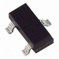
ADR370ART-R2 Analog Devices Inc, ADR370ART-R2 Datasheet - Page 8

ADR370ART-R2
Manufacturer Part Number
ADR370ART-R2
Description
IC REF PREC LO PWR 2.048V SOT-23
Manufacturer
Analog Devices Inc
Datasheet
1.ADR370ARTZ-REEL7.pdf
(12 pages)
Specifications of ADR370ART-R2
Rohs Status
RoHS non-compliant
Reference Type
Series
Voltage - Output
2.048V
Tolerance
±0.5%
Temperature Coefficient
100ppm/°C
Voltage - Input
2.3 ~ 15 V
Number Of Channels
1
Current - Quiescent
72µA
Current - Output
5mA
Operating Temperature
-40°C ~ 125°C
Mounting Type
Surface Mount
Package / Case
SOT-23-3, TO-236-3, Micro3™, SSD3, SST3
Current - Cathode
-
Other names
ADR370ART-R2TR
ADR370
THEORY OF OPERATION
The ADR370 uses the band gap concept to produce a stable,
low temperature coefficient voltage reference suitable for high
accuracy data acquisition components and systems. This device
makes use of the underlying temperature characteristics of a
silicon transistor’s base-emitter voltage (V
biased operating region. Under this condition, all such transistors
have a −2 mV/°C temperature coefficient (TC) and a V
when extrapolated to absolute zero, 0 K, (with collector current
proportional to absolute temperature), approximate the silicon
band gap voltage. By summing a voltage that has an equal and
opposite temperature coefficient of 2 mV/°C with a V
forward-biased transistor, an almost zero TC reference can be
developed. The simplified circuit diagram in Figure 12 shows
how a compensating voltage, V1, is achieved by driving two
transistors at different current densities and amplifying the
resulting V
sum (V
produce a stable reference voltage of 2.048 V at the output.
R3
R2
R1
BG
) of V
BE
difference (ΔV
V1
BE
and V1 is then buffered and amplified to
Figure 12. Simplified Schematic
R4
BE
, which has a positive TC). The
BE
) in the forward-
R5
V
R6
DS
V
V
GND
OUT
IN
BE
BE
of a
that,
Rev. C | Page 8 of 12
APPLYING THE ADR370
To achieve the specified performance, two external components
should be used in conjunction with the ADR370: a 4.7 μF capa-
citor and a 1 μF capacitor. The 4.7 μF capacitor should be applied
to the input, and the 1 μF capacitor should be applied to the
output. Figure 13 shows the ADR370 with both the input and
output capacitors attached.
For further transient response optimization, an additional 0.1 μF
capacitor in parallel with the 4.7 μF input capacitor can be used.
A 1 μF output capacitor provides stable performance for all
loading conditions. The ADR370 can, however, operate under
low (−100 μA < I
a 0.2 μF output capacitor and a 1 μF input capacitor.
Figure 13. Typical Connection Diagram
OUT
C
4.7µF
C
1µF
IN
OUT
< +100 μA) current conditions with just
V
V
IN
OUT
ADR370
GND


