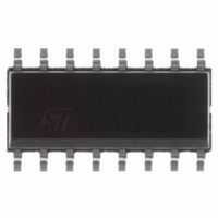
L6910GTR STMicroelectronics, L6910GTR Datasheet - Page 9

L6910GTR
Manufacturer Part Number
L6910GTR
Description
IC PWM BUCK BST VM 16SOIC
Manufacturer
STMicroelectronics
Datasheet
1.L6910GTR.pdf
(26 pages)
Specifications of L6910GTR
Pwm Type
Voltage Mode
Number Of Outputs
1
Frequency - Max
230kHz
Duty Cycle
100%
Voltage - Supply
5 V ~ 12 V
Buck
Yes
Boost
Yes
Flyback
No
Inverting
No
Doubler
No
Divider
No
Cuk
No
Isolated
No
Operating Temperature
-40°C ~ 150°C
Package / Case
16-SOIC (3.9mm Width)
Frequency-max
230kHz
Topology
Step Down
Output Voltage
0.9 V to 12 V
Output Current
1300 mA
Switching Frequency
50 KHz to 1000 KHz
Duty Cycle (max)
100 %
Maximum Operating Temperature
+ 150 C
Minimum Operating Temperature
- 40 C
Mounting Style
SMD/SMT
Synchronous Pin
No
Lead Free Status / RoHS Status
Lead free / RoHS Compliant
Other names
497-6111-2
Available stocks
Company
Part Number
Manufacturer
Quantity
Price
Part Number:
L6910GTR
Manufacturer:
ST
Quantity:
20 000
The response time to a load transient is different for the application or the removal of the load: if during the ap-
plication of the load the inductor is charged by a voltage equal to the difference between the input and the output
voltage, during the removal it is discharged only by the output voltage. The following expressions give approx-
imate response time for ∆I load transient in case of enough fast compensation network response:
The worst condition depends on the input voltage available and the output voltage selected. Anyway the worst
case is the response time after removal of the load with the minimum output voltage programmed and the max-
imum input voltage available.
4.7 Output Capacitor
The output capacitor is a basic component for the fast response of the power supply. In fact, during load tran-
sient, for first few microseconds they supply the current to the load. The controller recognizes immediately the
load transient and sets the duty cycle at 100%, but the current slope is limited by the inductor value. The output
voltage has a first drop due to the current variation inside the capacitor (neglecting the effect of the ESL):
A minimum capacitor value is required to sustain the current during the load transient without discharge it. The
voltage drop due to the output capacitor discharge is given by the following equation:
Where D
during load transient and the lower is the output voltage static ripple.
4.8 Input Capacitor
The input capacitor has to sustain the ripple current produced during the on time of the upper MOS, so it must
have a low ESR to minimize the losses. The rms value of this ripple is:
Where D is the duty cycle. The equation reaches its maximum value with D = 0.5. The losses in worst case are:
4.9 Compensation Network Design
The control loop is a voltage mode (figure 10). The output voltage is regulated to the input Reference voltage
level (EAREF). The error amplifier output V
a pulse-width modulated (PWM) wave with an amplitude of V
output filter. The modulator transfer function is the small-signal transfer function of V
has a double pole at frequency F
output capacitor ESR. The DC Gain of the modulator is simply the input voltage V
oscillator voltage ∆V
MAX
is the maximum duty cycle value that is 100%. The lower is the ESR, the lower is the output drop
OSC
.
t
application
∆
V
LC
OUT
depending on the L-C
=
---------------------------------------------------------------------------------------------
2 C
I
=
∆
rms
COMP
⋅
V
----------------------------- -
V
OUT
IN
P
OUT
=
L
is then compared with the oscillator triangular wave to provide
–
=
I
⋅
OUT
V
=
I ∆
⋅
ESR I
OUT
(
∆
V
I
∆
INMIN
OUT
D
I
⋅
2
OUT
out
⋅
2
rms
(
IN
⋅
resonance and a zero at F
1 D
t
ESR
⋅
removal
⋅
at the PHASE node. This wave is filtered by the
–
D
L
MAX
)
–
=
V
OUT
-------------- -
V
L
OUT
⋅
I ∆
)
IN
divided by the peak-to-peak
OUT
ESR
/V
COMP
depending on the
. This function
L6910G
9/26


