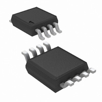
LM5021MM-1/NOPB National Semiconductor, LM5021MM-1/NOPB Datasheet - Page 7

LM5021MM-1/NOPB
Manufacturer Part Number
LM5021MM-1/NOPB
Description
IC PWM CTRLR AC-DC CURR 8-MSOP
Manufacturer
National Semiconductor
Datasheet
1.LM5021MM-1NOPB.pdf
(14 pages)
Specifications of LM5021MM-1/NOPB
Pwm Type
Current Mode
Number Of Outputs
1
Frequency - Max
1MHz
Duty Cycle
85%
Voltage - Supply
8 V ~ 30 V
Buck
Yes
Boost
Yes
Flyback
Yes
Inverting
Yes
Doubler
No
Divider
No
Cuk
No
Isolated
Yes
Operating Temperature
-40°C ~ 125°C
Package / Case
8-MSOP, Micro8™, 8-uMAX, 8-uSOP,
Frequency-max
1MHz
Lead Free Status / RoHS Status
Lead free / RoHS Compliant
Other names
LM5021MM-1
LM5021MM-1TR
LM5021MM-1TR
Available stocks
Company
Part Number
Manufacturer
Quantity
Price
Part Number:
LM5021MM-1/NOPB
Manufacturer:
TI/德州仪器
Quantity:
20 000
Detailed Operating Description
START UP CIRCUIT
Referring to
charged through the start-up resistor Rstart, when the recti-
fied ac input voltage HV is applied. The VIN current consumed
by the LM5021 is only 18 µA (nominal) while the capacitor
C
input voltage, VIN reaches the upper VIN UVLO threshold of
20V, the internal VCC linear regulator is enabled. The VCC
regulator will remain on until VIN falls to the lower UVLO
threshold of 7.25V (12.5V hysteresis). When the VCC regu-
lator is turned on, the external capacitor at the VCC pin begins
to charge. The PWM controller, soft-start circuit and gate driv-
er are enabled when the VCC voltage reaches the VCC UVLO
upper threshold of 7V. The VCC UVLO has 1.2V hysteresis
between the upper and lower thresholds to avoid chattering
during transients on the VCC pin. When the VCC UVLO en-
ables the switching power supply, energy is transferred from
the primary to the secondary transformer winding(s). A bias
winding, shown in
sustain the VCC regulator. The voltage supplied should be
VIN
is initially charged to the start-up threshold. When the
Output Switching Frequency vs RT
Figure
Figure
2, the input capacitor C
2, delivers power to the VIN pin to
FIGURE 2. Start-Up Circuit Block Diagram
VIN
20144210
is trickle
7
from 11V (VCC regulated voltage maximum plus VCC regu-
lator dropout voltage) to 30V (maximum operating VIN volt-
age). The bias winding should always be connected to the
VIN pin as shown in
to the VCC pin. The start-up sequence is completed and nor-
mal operation begins when the voltage from the bias winding
is sufficient to maintain VCC level greater than the VCC UVLO
threshold (5.8V typical).
The LM5021 is designed for ultra-low start-up current into the
VIN pin. To accomplish this very low start-up current, the VCC
regulator of the LM5021 is unique as compared to the VCC
regulator used in other controllers of the LM5xxx family. The
LM5021 is designed specifically for applications with the bias
winding connected to the VIN pin as shown in Figure 2. It is
not recommended that the bias winding be connected to
the VCC pin of the LM5021.
The size of the start-up resistor Rstart not only affects power
supply start-up time, but also power supply efficiency since
the resistor dissipates power in normal operation. The ultra
low start-up current of the LM5021 allows a large value Rstart
resistor (up to 3 MΩ) for improved efficiency with reasonable
start-up time.
Figure
2. Do not connect the bias winding
20144211
www.national.com


