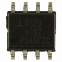
ISL6520ACBZ Intersil, ISL6520ACBZ Datasheet - Page 7

ISL6520ACBZ
Manufacturer Part Number
ISL6520ACBZ
Description
IC CNTRLR PWM SYNC BUCK 8SOIC
Manufacturer
Intersil
Datasheet
1.ISL6520ACBZ.pdf
(12 pages)
Specifications of ISL6520ACBZ
Pwm Type
Voltage Mode
Number Of Outputs
1
Frequency - Max
340kHz
Duty Cycle
100%
Voltage - Supply
4.5 V ~ 5.5 V
Buck
Yes
Boost
No
Flyback
No
Inverting
No
Doubler
No
Divider
No
Cuk
No
Isolated
No
Operating Temperature
0°C ~ 70°C
Package / Case
8-SOIC (3.9mm Width)
Frequency-max
340kHz
Input Voltage
5V
Output Voltage
5V
Frequency
300kHz
Supply Voltage Range
4.5V To 5.5V
Digital Ic Case Style
SOIC
No. Of Pins
8
Operating Temperature Range
0°C To +70°C
Filter Terminals
SMD
Rohs Compliant
Yes
Control Mode
Voltage
Lead Free Status / RoHS Status
Lead free / RoHS Compliant
Available stocks
Company
Part Number
Manufacturer
Quantity
Price
Part Number:
ISL6520ACBZ
Manufacturer:
INTERSIL
Quantity:
20 000
Company:
Part Number:
ISL6520ACBZ-T
Manufacturer:
INTERSIL
Quantity:
5 591
Part Number:
ISL6520ACBZ-T
Manufacturer:
INTERSIL
Quantity:
20 000
Figure 3 shows the critical power components of the converter.
To minimize the voltage overshoot, the interconnecting wires
indicated by heavy lines should be part of a ground or power
plane in a printed circuit board. The components shown in
Figure 3 should be located as close together as possible.
Please note that the capacitors C
represent numerous physical capacitors. Locate the ISL6520A
within 3 inches of the MOSFETs, Q
for the MOSFETs’ gate and source connections from the
ISL6520A must be sized to handle up to 1A peak current.
Figure 4 shows the circuit traces that require additional
layout consideration. Use single point and ground plane
construction for the circuits shown. Minimize any leakage
current paths on the COMP/OCSET pin and locate the
resistor, R
the internal current source is only 20µA. Provide local V
decoupling between VCC and GND pins. Locate the
capacitor, C
PHASE pins. All components used for feedback
compensation should be located as close to the IC a
practical.
Feedback Compensation
Figure 5 highlights the voltage-mode control loop for a
synchronous-rectified buck converter. The output voltage
(V
error amplifier (Error Amp) output (V
the oscillator (OSC) triangular wave to provide a
+5V
OUT
FIGURE 3. PRINTED CIRCUIT BOARD POWER AND
FIGURE 4. PRINTED CIRCUIT BOARD SMALL SIGNAL
ISL6520A
) is regulated to the Reference voltage level. The
COMP/OCSET
ISL6520A
OSCET
UGATE
PHASE
LGATE
BOOT
GND
GROUND PLANES OR ISLANDS
LAYOUT GUIDELINES
close to the COMP/OCSET pin because
as close as practical to the BOOT and
BOOT
PHASE
VCC
C
BOOT
Q
V
Q
+5V
RETURN
2
IN
1
7
C
D
VCC
IN
1
1
and C
and Q
E/A
C
O
) is compared with
IN
Q
2
+V
Q
may each
. The circuit traces
1
2
L
IN
O
L
C
O
O
C
O
V
OUT
V
CC
OUT
ISL6520A
pulse-width modulated (PWM) wave with an amplitude of
V
output filter (L
The modulator transfer function is the small-signal transfer
function of V
Gain and the output filter (L
break frequency at F
the modulator is simply the input voltage (V
peak-to-peak oscillator voltage ΔV
Modulator Break Frequency Equations
The compensation network consists of the error amplifier
(internal to the ISL6520A) and the impedance networks Z
and Z
a closed loop transfer function with the highest 0dB crossing
frequency (f
is the difference between the closed loop phase at f
180 degrees. The following equations relate the
compensation network’s poles, zeros and gain to the
components (R
these guidelines for locating the poles and zeros of the
compensation network:
F LC
ΔV
1. Pick Gain (R
2. Place 1
3. Place 2
IN
FIGURE 5. VOLTAGE-MODE BUCK CONVERTER
OSC
at the PHASE node. The PWM wave is smoothed by the
=
FB
------------------------------------------ -
2π x
. The goal of the compensation network is to provide
OSC
ST
ND
0dB
COMPARATOR
OUT
L O x C O
1
O
COMPENSATION DESIGN
Zero Below Filter’s Double Pole (~75% F
ERROR
AMP
DETAILED COMPENSATION COMPONENTS
V
Zero at Filter’s Double Pole.
ISL6520A
1
) and adequate phase margin. Phase margin
and C
E/A
, R
2
PWM
/V
/R
Z
+
E/A
-
2
1
FB
-
+
COMP
LC
, R
) for desired converter bandwidth.
O
C
. This function is dominated by a DC
REFERENCE
).
1
REFERENCE
and a zero at F
3
, C
C
+
2
-
O
1
DRIVER
DRIVER
R
F ESR
, C
and C
Z
2
IN
2
, and C
OSC
FB
=
O
Z
------------------------------------------- -
2π x ESR x C O
FB
), with a double pole
ESR
.
PHASE
(PARASITIC)
V
C
3
IN
3
) in Figure 7. Use
IN
L
Z
R
. The DC Gain of
1
O
IN
1
) divided by the
R
ESR
December 10, 2009
C
3
O
V
OUT
0dB
V
LC
FN9016.6
(EQ. 4)
OUT
and
).
IN


