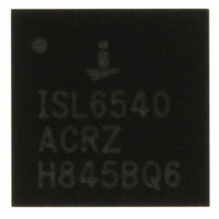
ISL6540ACRZ Intersil, ISL6540ACRZ Datasheet - Page 13

ISL6540ACRZ
Manufacturer Part Number
ISL6540ACRZ
Description
IC CTLR PWM BUCK 1PHASE 28-QFN
Manufacturer
Intersil
Datasheet
1.ISL6540ACRZ-T.pdf
(22 pages)
Specifications of ISL6540ACRZ
Pwm Type
Voltage Mode
Number Of Outputs
1
Frequency - Max
2MHz
Duty Cycle
100%
Voltage - Supply
2.97 V ~ 22 V
Buck
Yes
Boost
No
Flyback
No
Inverting
No
Doubler
No
Divider
No
Cuk
No
Isolated
No
Operating Temperature
0°C ~ 70°C
Package / Case
28-VQFN Exposed Pad, 28-HVQFN, 28-SQFN, 28-DHVQFN
Frequency-max
2MHz
Number Of Pwm Outputs
1
On/off Pin
No
Adjustable Output
Yes
Topology
Buck
Switching Freq
250 TO 2000kHz
Operating Supply Voltage (max)
5.5V
Output Current
4A
Output Voltage
0.6 to 20V
Synchronous Pin
No
Operating Temperature Classification
Commercial
Mounting
Surface Mount
Pin Count
28
Package Type
QFN EP
Rohs Compliant
YES
Lead Free Status / RoHS Status
Lead free / RoHS Compliant
Available stocks
Company
Part Number
Manufacturer
Quantity
Price
Company:
Part Number:
ISL6540ACRZ
Manufacturer:
Intersil
Quantity:
35
Part Number:
ISL6540ACRZ
Manufacturer:
ISL
Quantity:
20 000
point varies mainly due to the MOSFETs r
and system noise. To avoid overcurrent tripping in the
normal operating load range, find the R
resistor from the previous detailed equations with:
Frequency Programming
By tying a resistor to GND from FS pin, the switching
frequency can be set between 250kHz and 2MHz.
Oscillator/VFF
The Oscillator is a triangle waveform, providing for leading
and falling edge modulation. The bottom of the oscillator
waveform is set at 1.0V. The ramp's peak-to-peak amplitude
is determined from the voltage on the VFF (Voltage
Feed-Forward) pin. See Equation 6:
An internal RC filter of 233kΩ and 2pF (341kHz) provides
filtering of the VFF voltage. An external RC filter may be
required to augment this filter in the event that it is
insufficient to prevent noise injection or control loop
interactions. Voltages below 2.9V on the VFF pin may result
in undesirable operation due to extremely small peak to
peak oscillator waveforms. The oscillator waveform should
not exceed VCC -1.0V. For high VFF voltages the
internal/external 5.5V linear regulator should be used. 5.5V
on VCC provides sufficient headroom for 100% duty cycle
operation when using the maximum VFF voltage of 22V. In
the event of sustained 100% duty cycle operation, defined as
32-clock cycles where no LG pulse is detected, LG will be
pulsed on to refresh the design’s bootstrap capacitor.
ΔVosc
1. Maximum r
2. Minimum I
3. Determine the overcurrent trip point greater than the
page 8.
maximum output continuous current at maximum
inductor ripple current.
=
0.16 VFF
LSOC
•
DS(ON)
and/or I
at the highest junction temperature.
HSOC
13
from specification table on
HSOC
DS(ON)
and/or R
variations
(EQ. 6)
LSOC
ISL6540A
Internal Series Linear Regulator
The VIN pin is connected to PVCC with a 2Ω internal series
linear regulator, which is internally compensated. The
external series linear regulator option should be used for
applications requiring pass elements of less than 2Ω. When
using the internal regulator, the LIN_DRV pin should be
connected directly to GND. The PVCC and VIN pins should
have a bypass capacitor (at least 10µF on PVCC is required)
connected to PGND. For proper operation the PVCC
capacitor must be within 150 mils of the PVCC and the
PGND pins, and be connected to these pins with dedicated
traces. The internal series linear regulator’s input (VIN) can
range between 3.3V to 20V ±10%. The internal linear
regulator is to provide power for both the internal MOSFET
drivers through the PVCC pin and the analog circuitry
through the VCC pin. The VCC pin should be connected to
the PVCC pin with an RC filter to prevent high frequency
driver switching noise from entering the analog circuitry.
When VIN drops below 5.5V, the pass element will saturate;
PVCC will track VIN, minus the dropout of the linear
regulator: PVCC = VIN-2xI
5V supply, the VIN pin should be tied directly to PVCC.
At start-up (PVCC = 0V and VIN = 0V) the DV/DT on VIN
should be kept below 1V/µs to prevent electrical overstress
on PVCC. Care should be taken to keep the DV/DT on VIN
below 0.05V/µs if the initial steady state voltage on PVCC is
above 2.0V, as electrical overstress on PVCC is otherwise
possible.
External Series Linear Regulator
The LIN_DRV pin provides sinking drive capability for an
external pass element linear regulator controller. The
external linear options are especially useful when the
Fs Hz
80
60
40
30
20
10
7
5
[
200k
]
FIGURE 4. R
≈
1.178
300k
×10
10
400k
FS
•
R
RESISTANCE vs FREQUENCY
FREQUENCY (Hz)
T
[ ]
VIN
Ω
–
600k
. When used with an external
0.973
800k
(R
T
1M
TO GND)
October 7, 2008
(EQ. 7)
FN6288.5
2M


