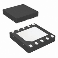
LM5033SD/NOPB National Semiconductor, LM5033SD/NOPB Datasheet - Page 10

LM5033SD/NOPB
Manufacturer Part Number
LM5033SD/NOPB
Description
IC CTRLR PWM PUSH PULL HV 10LLP
Manufacturer
National Semiconductor
Series
PowerWise®r
Datasheet
1.LM5033MMNOPB.pdf
(17 pages)
Specifications of LM5033SD/NOPB
Pwm Type
Voltage Mode
Number Of Outputs
2
Frequency - Max
1MHz
Duty Cycle
95.5%
Voltage - Supply
15 V ~ 90 V
Buck
Yes
Boost
Yes
Flyback
No
Inverting
Yes
Doubler
No
Divider
No
Cuk
No
Isolated
No
Operating Temperature
-40°C ~ 125°C
Package / Case
10-LLP
Frequency-max
1MHz
For Use With
LM5033SD-EVAL - BOARD EVALUATION LM5033SD
Lead Free Status / RoHS Status
Lead free / RoHS Compliant
Other names
LM5033SD
LM5033SDTR
LM5033SDTR
Available stocks
Company
Part Number
Manufacturer
Quantity
Price
www.national.com
Application Information
V
The voltage applied at pin 1, normally the same as that
applied to the main transformer’s primary, can be in the
range of 15 to 90V, with transient capability to 100V. The
current into pin 1 depends not only on V
load on the output driver pins, any load on V
or not an external voltage is applied to V
the absolute maximum rating of the LM5033, it is recom-
mended the circuit of Figure 2 be used to filter transients
which may occur at the input supply.
If V
currents for the LM5033, and output driver currents, to be
supplied at Vin and through the internal regulator, the re-
quired input current (Iin) is shown in the Typical Performance
Characteristics (I
If V
shown in the above mentioned graph until the external volt-
age is applied to V
the outputs are enabled and load current begins to flow. The
current into Vin will then drop to a nominal 150µA (Pin 10 =
open or grounded).
V
The capacitor at the V
and stability, but also a necessary time delay during start-up.
The time delay allows the internal circuitry of the LM5033,
and associated external circuitry, to stabilize before V
reaches its final value, at which time the outputs are enabled
and the softstart sequence begins. Any external circuitry
connected to the REF output (Pin 2) and Softstart (Pin 10)
should be designed to stabilize during the time delay.
The current limit of the V
capacitor, determine the V
1µF capacitor will provide approximately 300 µs of delay,
with larger capacitors providing proportionately longer de-
IN
CC
CC
CC
(PIN 1)
(PIN 4)
is not powered externally, requiring all internal bias
is powered externally, Iin will increase with V
FIGURE 2. Input Transient Protection
IN
CC
vs. V
. In most applications, this occurs once
CC
IN
pin provides not only noise filtering
).
CC
CC
turn-on time delay. Typically, a
regulator, and the external
CC
IN
(Continued)
. If Vin is close to
, but also on the
CC
20035415
, and whether
IN
CC
as
10
lays. Experimentation with the final design may be neces-
sary to determine the minimum value for the V
SOFTSTART (PIN 10)
The capacitor at pin 10 determines the time required for the
output duty cycle to increase from zero to the final value for
regulation. The minimum acceptable time is dependent on
the response of the feedback loops to the COMP pin, as well
as the characteristics of the magnetic components. If the
Softstart time is too quick, the system output could signifi-
cantly overshoot its intended voltage before the loop has a
chance to establish regulation, possibly adversely affecting
the load. Experimentation with the final design is usually
necessary to determine the minimum value for the SS ca-
pacitor.
CURRENT SENSE (PIN 8)
This pin typically receives an input representative of the
primary current from the current sense elements of the ex-
ternal circuitry. The peak amplitude at this pin must be less
than 0.5V for normal operation. Filtering at this pin should be
sufficient to prevent false triggering of the Current Sense
comparator, but not significantly delay detection of an over-
current condition. The filter’s capacitor at pin 8 should not be
larger than 2200 pF.
OSCILLATOR, SYNC INPUT (PIN 9)
The internal oscillator frequency is generally selected in
conjunction with the system magnetic components, and any
other aspects of the system which may be affected by the
frequency. The R
ing to the formula in the Functional Description. Each output
(OUT1 and OUT2) switches at half the oscillator frequency. If
the required frequency value is critical in a particular appli-
cation, the tolerance of the external resistor, and the fre-
quency tolerance indicated in the Electrical Characteristics,
must be taken into account when selecting the resistor.
If the LM5033 is to be synchronized to an external clock, that
signal must be coupled into pin 9 through a 100 pF capacitor.
The R
selected to set the internal oscillator to a frequency lower
than the external synchronizing frequency. The amplitude of
the external pulses must take pin 9 above 3.8V on the
low-to-high transition but no higher than 5.5V. The clock
pulse width should be between 15 and 150 ns.
DEADTIME ADJUSTMENT
If the application requires a change in the minimum dead-
time between the outputs, the circuits in Figure 3 are recom-
mended. Suggested values for the resistor and capacitor at
each output are 500Ω, and 100 pF, respectively for a nomi-
nal 50 ns change. The diodes can be 1N4148, or similar.
t
resistor is still required in this case, and it must be
t
resistor at pin 9 sets the frequency accord-
CC
capacitor.


