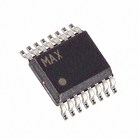
MAX8554EEE+ Maxim Integrated Products, MAX8554EEE+ Datasheet - Page 2

MAX8554EEE+
Manufacturer Part Number
MAX8554EEE+
Description
IC CNTRLR BUCK PWM 16-QSOP
Manufacturer
Maxim Integrated Products
Datasheet
1.MAX8553EEE.pdf
(24 pages)
Specifications of MAX8554EEE+
Pwm Type
Controller
Number Of Outputs
1
Frequency - Max
550kHz
Duty Cycle
95%
Voltage - Supply
4.5 V ~ 28 V
Buck
Yes
Boost
No
Flyback
No
Inverting
No
Doubler
No
Divider
Yes
Cuk
No
Isolated
No
Operating Temperature
-40°C ~ 85°C
Package / Case
16-QSOP
Frequency-max
550kHz
Output Voltage
0.6 V to 3.5 V
Output Current
25000 mA
Mounting Style
SMD/SMT
Switching Frequency
550 KHz
Maximum Operating Temperature
+ 85 C
Minimum Operating Temperature
- 40 C
Synchronous Pin
No
Topology
Buck
Dc
0649
Lead Free Status / RoHS Status
Lead free / RoHS Compliant
ABSOLUTE MAXIMUM RATINGS
V+, EN/HSD, EN, HSD to GND...............................-0.3V to +30V
PGND to GND .......................................................-0.3V to +0.3V
VTT, REFIN, POK, OUT, FB, VL to GND...................-0.3V to +6V
REF, VTTR, DL, ILIM, FSEL to GND ............-0.3V to (V
LX to PGND ...............................................................-2V to +30V
BST to GND ............................................................-0.3V to +36V
DH to LX ...................................................................-0.3V to +6V
LX to BST..................................................................-6V to +0.3V
4.5V to 28V Input, Synchronous PWM Buck Controllers
for DDR Termination and Point-of-Load Applications
ELECTRICAL CHARACTERISTICS
(V
PGND = LX = GND, BST = VL, T
Stresses beyond those listed under “Absolute Maximum Ratings” may cause permanent damage to the device. These are stress ratings only, and functional
operation of the device at these or any other conditions beyond those indicated in the operational sections of the specifications is not implied. Exposure to
absolute maximum rating conditions for extended periods may affect device reliability.
2
V+ Input Voltage Range
V+ Input Voltage Range
EN/HSD Input Voltage Range
EN Input Voltage Range
EN Input Current
HSD Input Voltage Range
HSD Input Current
REFIN Input Voltage Range
V+ Supply Current (MAX8553)
V+ Supply Current (MAX8554)
REFIN Supply Current
EN/HSD Supply Current
VL Supply Current
V+ Shutdown Supply Current
REFIN Shutdown Supply Current
VL Shutdown Supply Current
VL Undervoltage-Lockout Threshold
VTT
VTT Input Bias Current
VTT Feedback Voltage Range
VTT Feedback Voltage Accuracy
FB Input Bias Current
V+
_______________________________________________________________________________________
= V
HSD
PARAMETER
= +12V, V
EN/HSD
= V
A
= 0°C to +85°C. Typical values are at T
REFIN
VL not connected to V+
VL connected to V+
MAX8553 enabled
MAX8554 enabled
MAX8554 enabled
V
V
V
EN/HSD = GND
EN/HSD = GND
V
Rising edge, typical hysteresis = 40mV
V
V
V
MAX8554, V
VTT
FB
VL
VL
VTT
REFIN
REFIN
= +2.5V, V
= V
= V
= 630mV
= +1.35V
= +1.25V
= V
= V
V+
V+
= 5.5V, V
= +5.5V, V
EN/HSD
EN/HSD
FB
VL
EN
= +600mV
+ 0.3V)
= +5V, C
= +1.8V
= +3.6V
VTT
CONDITIONS
EN/HSD
= +1.35V
VL
= 0V
= 4.7µF, C
REF Short Circuit to GND ...........................................Continuous
Continuous Power Dissipation (T
Operating Temperature Range ...........................-40°C to +85°C
Junction Temperature ......................................................+150°C
Storage Temperature Range .............................-65°C to +150°C
Lead Temperature (soldering, 10s) .................................+300°C
16-Pin QSOP (derated 8.3mW/°C above +70°C) ........667mW
A
= +25°C, unless otherwise specified.)
VTTR
= 1µF, C
REF
-0.15
-0.15
MIN
4.05
49.5
49.5
4.5
1.5
1.5
1.5
= 0.22µF, V
6
0
0
A
= +70°C)
TYP
0.62
4.25
125
0.8
0.8
20
50
50
2
5
3
5
FSEL
MAX
= 0V, ILIM = VL,
28.0
28.0
28.0
0.90
4.40
50.5
50.5
250
5.5
3.6
1.2
1.2
1.8
28
40
10
12
3
5
1
0
0
% V
UNITS
mA
mA
mA
µA
µA
µA
µA
µA
µA
µA
µA
µA
V
V
V
V
V
V
V
V
RE FIN


