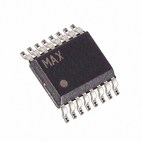
MAX8554EEE+ Maxim Integrated Products, MAX8554EEE+ Datasheet - Page 22

MAX8554EEE+
Manufacturer Part Number
MAX8554EEE+
Description
IC CNTRLR BUCK PWM 16-QSOP
Manufacturer
Maxim Integrated Products
Datasheet
1.MAX8553EEE.pdf
(24 pages)
Specifications of MAX8554EEE+
Pwm Type
Controller
Number Of Outputs
1
Frequency - Max
550kHz
Duty Cycle
95%
Voltage - Supply
4.5 V ~ 28 V
Buck
Yes
Boost
No
Flyback
No
Inverting
No
Doubler
No
Divider
Yes
Cuk
No
Isolated
No
Operating Temperature
-40°C ~ 85°C
Package / Case
16-QSOP
Frequency-max
550kHz
Output Voltage
0.6 V to 3.5 V
Output Current
25000 mA
Mounting Style
SMD/SMT
Switching Frequency
550 KHz
Maximum Operating Temperature
+ 85 C
Minimum Operating Temperature
- 40 C
Synchronous Pin
No
Topology
Buck
Dc
0649
Lead Free Status / RoHS Status
Lead free / RoHS Compliant
Use R
where I
determined by:
where R
tance (1.4Ω typ) and R
tance of the MOSFET (~2Ω):
where V
When the MAX8553 is sinking current, the high-side
MOSFET operates as a zero-voltage switch and the
low-side MOSFETs operate as a nonzero-voltage
switch.
In addition to the losses above, allow about 20% more
for additional losses due to MOSFET output capaci-
tances and low-side MOSFET body-diode reverse
recovery charge dissipated in the high-side MOSFET
that is not well defined in the MOSFET data sheet. Refer
to the MOSFET data sheet for thermal-resistance speci-
fications to calculate the PC board area needed to
maintain the desired maximum operating junction tem-
perature with the above calculated power dissipations.
To reduce EMI caused by switching noise, add a 0.1µF
ceramic capacitor from the high-side switch drain to
the low-side switch source, or add resistors in series
with DH and DL to slow down the switching transitions.
Adding series resistors increases the power dissipation
of the MOSFET, so ensure that this does not overheat
the MOSFET.
4.5V to 28V Input, Synchronous PWM Buck Controllers
for DDR Termination and Point-of-Load Applications
22
______________________________________________________________________________________
DS(ON)
GATE
GS
DH
P
P
P
HSCC
HSSW
HSDR
= V
is the high-side MOSFET driver’s on-resis-
at T
is the average DH driver output current
VL
=
=
=
I
J(MAX)
GATE
V
V
= 5V.
Q
V
IN
OUT
G
IN
×
×
I
LOAD
=
V
:
GATE
×
GS
R
DH
(
I
×
LOAD
×
f
2 5 .
S
+
is the internal gate resis-
f
S
R
×
V
×
GATE
R
)
2
Q
GATE
GS
R
×
I
GATE
GATE
R
+
DS ON
+
Q
R
(
GD
DH
)
Power dissipation in the MAX8553/MAX8554 IC is pri-
marily due to the on-chip MOSFETs’ gate drivers (DH
and DL). This power dissipation depends on the gate
charge of the external MOSFETs used. Power dissipa-
tion in the MAX8553 also depends on the VTTR load
current (I
the power dissipation:
where Q
high-side and low-side MOSFETs, respectively. Select
the switching frequency and V
the power dissipation does not exceed the package
power-dissipation requirement.
A properly designed PC board layout is important in
any switching regulator. The switching power stage
requires particular attention. If possible, mount all the
power components on the top-side of the board with
their ground terminals flush against one another. Follow
these guidelines for good PC board layout:
1) Keep the high-current paths short, especially at the
2) Connect GND and PGND together at a single point.
3) Keep the power traces and load connections short.
4) LX and PGND connections to the low-side MOSFET
ground terminals. This practice is essential for sta-
ble, low-jitter operation.
This practice is essential for high efficiency. The use
of thick copper PC boards (2oz vs. 1oz) can notice-
ably enhance full-load efficiency. Correctly routing
PC board traces is a difficult task that must be
approached in terms of fractions of centimeters,
where a single mΩ of excess trace resistance caus-
es a measurable efficiency penalty.
for current limiting must be made using Kelvin-
sense connections in order to guarantee the cur-
rent-limit accuracy. With 8-pin SO MOSFETs, this
can be done by routing power to the MOSFETs from
P
GH
VTTR
D
=
and Q
(
). Use the following equation to calculate
V
V
Applications Information
+
)
Control IC Power Dissipation
×
GL
[
f
S
are the total gate charge of the
×
(
Q
GH
+
V+
Q
PC Board Layout
GL
correctly to ensure
)
+
I
VTTR
]


