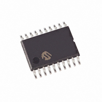
MCP1631HV-500E/ST Microchip Technology, MCP1631HV-500E/ST Datasheet - Page 17

MCP1631HV-500E/ST
Manufacturer Part Number
MCP1631HV-500E/ST
Description
IC INTEGRATED PWM HS 20TSSOP
Manufacturer
Microchip Technology
Datasheets
1.MCP1631VHVT-330EST.pdf
(34 pages)
2.MCP1631VHVT-330EST.pdf
(32 pages)
3.MCP1631HV-330EST.pdf
(54 pages)
4.MCP1631-EST.pdf
(32 pages)
Specifications of MCP1631HV-500E/ST
Package / Case
20-TSSOP
Pwm Type
Current Mode
Number Of Outputs
1
Frequency - Max
2MHz
Duty Cycle
10%
Voltage - Supply
3.5 V ~ 16 V
Buck
Yes
Boost
No
Flyback
No
Inverting
No
Doubler
No
Divider
No
Cuk
No
Isolated
Yes
Operating Temperature
-40°C ~ 125°C
Frequency-max
2MHz
Output Voltage
3.3 V to 5 V
Output Current
250 mA
Input Voltage
3 V to 5.5 V
Switching Frequency
2 MHz
Operating Temperature Range
- 40 C to + 125 C
Mounting Style
SMD/SMT
Frequency
1MHz
Digital Ic Case Style
TSSOP
No. Of Pins
20
Peak Reflow Compatible (260 C)
Yes
Rohs Compliant
Yes
Leaded Process Compatible
Yes
Lead Free Status / RoHS Status
Lead free / RoHS Compliant
For Use With
MCP1631RD-DCPC1 - REF DES BATT CHARG OR LED DRIVERMCP1631RD-MCC2 - REFERENCE DESIGN MCP1631HV
Lead Free Status / Rohs Status
Lead free / RoHS Compliant
4.0
4.1
The MCP1631/MCP1631V device family combines the
analog functions to develop high frequency switch
mode power systems while integrating features for
battery charger and LED current source applications.
With the integration of a MOSFET driver, voltage
sense, current sense and over voltage protection, the
MCP1631/MCP1631V is a highly integrated, high-
speed analog pulse width modulator.
The MCP1631/MCP1631V output (V
control the switch of the power system (on and off
time). By controlling the switch on and off time, the
power system output can be regulated. With the
oscillator and reference voltage as inputs, a simple
interface to a microcontroller is available with the
MCP1631/MCP1631V to develop intelligent power
systems. A good example of an intelligent power
system is a battery charger, programmable LED driver
current source or programmable power supply.
The MCP1631/MCP1631V is a combination of
specialty analog blocks consisting of a Pulse Width
Modulator (PWM), MOSFET Driver, Current Sense
Amplifier
Overvoltage Comparator (C2) and additional features
(Shutdown, Undervoltage Lockout, Overtemperature
Protection). For the HV options, an internal low dropout
regulator is integrated for operation from high voltage
inputs (MCP1631HV/MCP1631VHV).
4.2
The internal PWM of the MCP1631/MCP1631V is
comprised of an error amplifier, high-speed comparator
and latch. The output of the amplifier is compared to
either the MCP1631 CS (primary current sense input)
or the MCP1631V V
the high speed comparator. When the CS or VRAMP
signal reach the level of the error amplifier output, the
on cycle is terminated and the external switch is
latched off until the beginning of the next cycle (high to
low transition of OSC
4.3
The MCP1631/MCP1631V output can be used to drive
the external MOSFET directly for low side topology
applications. The V
700 mA and sinking up to 1A of current from a P
source of 5V. Typical output power using the V
output to directly drive the external MOSFET can
exceed 50W depending upon application and switching
frequency.
© 2008 Microchip Technology Inc.
DETAILED DESCRIPTION
Device Overview
Pulse Width Modulator (PWM)
V
EXT
(A2),
MOSFET Driver
Voltage
RAMP
EXT
IN
).
is capable of sourcing up to
(voltage mode ramp input) of
Sense
Amplifier
EXT
) is used to
MCP1631/HV/MCP1631V/VHV
(A3),
VDD
EXT
4.4
The A2 current sense amplifier is used to sense current
in the secondary side of a SEPIC converter or
freewheeling current in a Buck converter. The inverting
amplifier has a built in voltage gain of ten with low offset
and high speed.
4.5
The A3 voltage sense amplifier is used to sense battery
voltage. In battery powered applications, it is important
to minimize the steady stage load current draw on the
battery. The voltage sense amplifier (A3) is used to
buffer a high impedance series divider used to reduce
the battery pack voltage to a level that can be read
using an analog to digital converter. The voltage sense
amplifier draws a very low quiescent current and
remains functional when the MCP1631/MCP1631V is
shutdown making it possible to read battery voltage
without turning on the charger.
4.6
The C2 overvoltage comparator is used to prevent the
power system from being damaged when the load
(battery) is disconnected. By comparing the divided
down power train output voltage with a 1.2V internal
reference voltage, the MCP1631/MCP1631V V
output switching is interrupted when the output voltage
is above a pre-set value. This limits the output voltage
of the power train, the 0V comparator’s hysteresis will
operate as a ripple regulator.
4.7
The MCP1631/MCP1631V shutdown feature is used to
disable the device with the exception of the voltage
sense amplifier A3 to minimize quiescent current draw.
While shutdown, A3 remains operational while the
device draws 4.4 µA from the input.
4.8
The MCP1631/MCP1631V has built in Undervoltage
Lockout (UVLO) that ensures the output V
forced to a known state (low) when the input voltage or
A
main MOSFET switch from being turned on during a
power up or down sequence.
The
shutdown protection feature, if the internal junction
temperature of the device becomes high, the
overtemperature protection feature will disable (pull the
V
VDD
EXT
output low) and shut down the power train.
is below the specified value. This prevents the
MCP1631/MCP1631V
Current Sense Amplifier (A2)
Voltage Sense Amplifier (A3)
Overvoltage Comparator(C2)
Shutdown Input
Protection
provides
DS22063B-page 17
a
EXT
thermal
pin is
EXT


