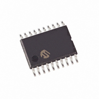
MCP1631HV-500E/ST Microchip Technology, MCP1631HV-500E/ST Datasheet - Page 9

MCP1631HV-500E/ST
Manufacturer Part Number
MCP1631HV-500E/ST
Description
IC INTEGRATED PWM HS 20TSSOP
Manufacturer
Microchip Technology
Datasheets
1.MCP1631VHVT-330EST.pdf
(34 pages)
2.MCP1631VHVT-330EST.pdf
(32 pages)
3.MCP1631HV-330EST.pdf
(54 pages)
4.MCP1631-EST.pdf
(32 pages)
Specifications of MCP1631HV-500E/ST
Package / Case
20-TSSOP
Pwm Type
Current Mode
Number Of Outputs
1
Frequency - Max
2MHz
Duty Cycle
10%
Voltage - Supply
3.5 V ~ 16 V
Buck
Yes
Boost
No
Flyback
No
Inverting
No
Doubler
No
Divider
No
Cuk
No
Isolated
Yes
Operating Temperature
-40°C ~ 125°C
Frequency-max
2MHz
Output Voltage
3.3 V to 5 V
Output Current
250 mA
Input Voltage
3 V to 5.5 V
Switching Frequency
2 MHz
Operating Temperature Range
- 40 C to + 125 C
Mounting Style
SMD/SMT
Frequency
1MHz
Digital Ic Case Style
TSSOP
No. Of Pins
20
Peak Reflow Compatible (260 C)
Yes
Rohs Compliant
Yes
Leaded Process Compatible
Yes
Lead Free Status / RoHS Status
Lead free / RoHS Compliant
For Use With
MCP1631RD-DCPC1 - REF DES BATT CHARG OR LED DRIVERMCP1631RD-MCC2 - REFERENCE DESIGN MCP1631HV
Lead Free Status / Rohs Status
Lead free / RoHS Compliant
2.0
Note:
for typical values = +25°C.
FIGURE 2-1:
Temperature.
FIGURE 2-2:
Hysteresis vs. Temperature.
FIGURE 2-3:
Temperature.
© 2008 Microchip Technology Inc.
Note:
0.068
0.067
0.066
0.065
0.064
0.063
0.062
0.061
2.89
2.88
2.87
2.86
2.85
2.84
2.83
2.82
2.81
4.00
3.80
3.60
3.40
3.20
3.00
2.80
Unless otherwise noted, V
2.8
TYPICAL PERFORMANCE CURVES
The graphs and tables provided following this note are a statistical summary based on a limited number of
samples and are provided for informational purposes only. The performance characteristics listed herein are
not tested or guaranteed. In some graphs or tables, the data presented may be outside the specified
operating range (e.g., outside specified power supply range) and therefore outside the warranted range.
V
DD
Device Turn Off
Device Turn On
= +5.0V
Ambient Temperature (°C)
Ambient Temperature (°C)
Ambient Temperature (°C)
Undervoltage Lockout vs.
Undervoltage Lockout
Input Quiescent Current vs.
V
DD
V
DD
= +3.3V
= +3.0V
IN
= 3.0V to 5.5V, F
V
DD
= +4.0V
V
DD
= +5.5V
OSC
MCP1631/HV/MCP1631V/VHV
= 1 MHz with 10% Duty Cycle, C
FIGURE 2-4:
Temperature (MCP1631/MCP1631V).
FIGURE 2-5:
vs. Temperature.
FIGURE 2-6:
Threshold vs. Temperature.
4.00
3.70
3.40
3.10
2.80
2.50
2.20
1.90
1.60
1.30
1.00
1.60
1.50
1.40
1.30
1.20
1.10
1.00
1.70
1.60
1.50
1.40
1.30
1.20
1.10
1.00
0.90
0.80
V
V
DD
DD
IN
= +3.3V
= +3.0V
V
V
DD
= 0.1 µF, V
DD
Ambient Temperature (°C)
Ambient Temperature (°C)
= +3.0V
= +3.3V
Ambient Temperature (°C)
V
DD
Shutdown Current vs.
Oscillator Input Threshold
Oscillator Disable Input
V
= +3.3V
DD
V
= +4.0V
DD
IN
= +4.0V
for typical values = 5.0V, T
V
V
DD
DD
V
= +5.0V
= +4.0V
V
DD
DD
V
= +5.0V
DD
= +3.0V
DS22063B-page 9
= +5.0V
V
V
V
DD
DD
DD
= +5.5V
= +5.5V
= +5.5V
A


