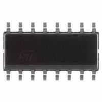
L6910G STMicroelectronics, L6910G Datasheet - Page 15

L6910G
Manufacturer Part Number
L6910G
Description
IC PWM BUCK BST VM 16SOICN
Manufacturer
STMicroelectronics
Datasheet
1.L6910GTR.pdf
(26 pages)
Specifications of L6910G
Pwm Type
Voltage Mode
Number Of Outputs
1
Frequency - Max
230kHz
Duty Cycle
100%
Voltage - Supply
5 V ~ 12 V
Buck
Yes
Boost
Yes
Flyback
No
Inverting
No
Doubler
No
Divider
No
Cuk
No
Isolated
No
Operating Temperature
-40°C ~ 150°C
Package / Case
16-SOIC (3.9mm Width)
Frequency-max
230kHz
Topology
Step Down
Output Voltage
0.9 V to 12 V
Output Current
1300 mA
Switching Frequency
50 KHz to 1000 KHz
Duty Cycle (max)
100 %
Maximum Operating Temperature
+ 150 C
Minimum Operating Temperature
- 40 C
Mounting Style
SMD/SMT
Synchronous Pin
No
Lead Free Status / RoHS Status
Lead free / RoHS Compliant
Available stocks
Company
Part Number
Manufacturer
Quantity
Price
Part Number:
L6910G
Manufacturer:
ST
Quantity:
20 000
Part Number:
L6910GTR
Manufacturer:
ST
Quantity:
20 000
6.5 APPLICATION SUGGESTIONS FOR HIGHER CURRENTS
For higher output currents, up to 20A, the following configuration can be used (with reference to the demo board
schematic):
Q1,Q2,Q3: STS11NF30L
Q4,Q5,Q6: STS17NF3LL
L: 2.5µH Magnetic 77121A7 Core 7T 2x AWG16
In these conditions, the following performance have been achieved:
Table 8.
For currents higher than 20A, bigger mosfets should be selected (e.g. STS25NH3LL) both for the high side and
low side (depending on the duty cycle and input voltage).
7
A compact demo board has been realized to manage currents in the range of 5A-6A .
The external power mosfets are included in a single SO8 package to save space and increase power density.
Two separate rails are provided, for V
The PGOOD signal is used as a logic level and it's been pulled up to V
voltage available on the demo board. In case of input voltage higher than 7V (PGOOD Pin Maximum Ab-
solute Rating) a 5V reference is required.
Figure 17. 6A Demo Board Schematic
GNDCC
GNDCC
GNDIN
GNDIN
GNDIN
V
VCC
VCC
VIN
VIN
IN
6A DEMO BOARD DESCRIPTION
5
5
5
5
5
(V)
V
OUT
1.2
1.5
1.8
2.5
3.3
(V)
C9
C9
C9
C8
C8
J1
J1
R6
R6
R10
R10
I
OUT
20
20
20
20
20
C5
C5
(A)
EAREF
EAREF
D1
D1
GND
GND
VCC
VCC
OSC
OSC
SS
SS
CC
COMP
COMP
15
15
7
7
4
4
2
2
8
8
and V
12
12
5
5
L6910
L6910
BOOT
BOOT
C19
C19
η (%)
U1
U1
81
83
85
89
91
C18
C18
R7
R7
IN
3
3
R5
R5
. They can be connected together by shorting the jumper J1.
R1
R1
OCSET
OCSET
6
6
VFB
VFB
11
11
10
10
14
14
13
13
C7
C7
9
9
1
1
VREF
VREF
PGND
PGND
UGATE
UGATE
PHASE
PHASE
LGATE
LGATE
PGOOD
PGOOD
C6
C6
V
IN
12
12
12
12
12
12
R8
R8
R9
R9
(V)
R4
R4
R4
Q1/Q1
Q1/Q1
Q2/Q1
Q2/Q1
R3
R3
IN
C20
C20
C20
V
because there's no other appropriate
D2
D2
OUT
1.2
1.5
1.8
2.5
3.3
5
(V)
R11
R11
C10
C10
L1
L1
I
OUT
C3-4
C3-4
20
20
20
20
20
20
C1- C2
C1- C2
(A)
R2
R2
L6910G
η (%)
VOUT
VOUT
GNDOUT
GNDOUT
PWRGD
PWRGD
80
83
85
88
91
93
15/26


