LM5025AMTCX/NOPB National Semiconductor, LM5025AMTCX/NOPB Datasheet - Page 11
LM5025AMTCX/NOPB
Manufacturer Part Number
LM5025AMTCX/NOPB
Description
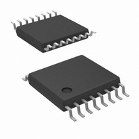
IC CTLR PWM CLAMP VOLT 16TSSOP
Manufacturer
National Semiconductor
Series
PowerWise®r
Datasheet
1.LM5025ASDNOPB.pdf
(16 pages)
Specifications of LM5025AMTCX/NOPB
Pwm Type
Voltage Mode
Number Of Outputs
2
Frequency - Max
1MHz
Duty Cycle
92.5%
Voltage - Supply
13 V ~ 90 V
Buck
Yes
Boost
Yes
Flyback
Yes
Inverting
Yes
Doubler
No
Divider
No
Cuk
No
Isolated
Yes
Operating Temperature
-40°C ~ 125°C
Package / Case
16-TSSOP
Frequency-max
1MHz
For Use With
LM5025AEVAL - BOARD EVALUATION LM5025ALM5025EVAL - EVALUATION BOARD FOR LM5025
Lead Free Status / RoHS Status
Lead free / RoHS Compliant
Other names
LM5025AMTCX
Available stocks
Company
Part Number
Manufacturer
Quantity
Price

Part Number:
LM5025AMTCX/NOPB
Manufacturer:
TI/德州仪器
Quantity:
20 000


charging the SS capacitor protects a continuously over-load-
ed converter with a low duty cycle hiccup mode.
These two modes of over-current protection allow the user
great flexibility to configure the system behavior in over-load
conditions. If it is desired for the system to act as a current
source during an over-load, then the CS1 cycle-by-cycle cur-
rent limiting should be used. In this case the current sense
signal should be applied to the CS1 input and the CS2 input
should be grounded. If during an overload condition it is de-
sired for the system to briefly shutdown, followed by softstart
retry, then the CS2 hiccup current limiting mode should be
used. In this case the current sense signal should be applied
to the CS2 input and the CS1 input should be grounded. This
shutdown / soft-start retry will repeat indefinitely while the
over-load condition remains. The hiccup mode will greatly re-
duce the thermal stresses to the system during heavy over-
loads. The cycle-by-cycle mode will have higher system
thermal dissipations during heavy overloads, but provides the
advantage of continuous operation for short duration overload
conditions.
It is possible to utilize both over-current modes concurrently,
whereby slight overload conditions activate the CS1 cycle-by-
cycle mode while more severe overloading activates the CS2
hiccup mode. Generally the CS1 input will always be config-
ured to monitor the main switch FET current each cycle. The
CS2 input can be configured in several different ways de-
pending upon the system requirements.
a) The CS2 input can also be set to monitor the main switch
FET current except scaled to a higher threshold than CS1
b) An external over-current timer can be configured which
trips after a pre-determined over-current time, driving the CS2
input high, initiating a hiccup event.
Oscillator and Sync Capability
The LM5025A oscillator is set by a single external resistor
connected between the RT pin and GND. To set a desired
oscillator frequency (F), the necessary RT resistor can be
calculated from:
where F is in kHz and RT in kΩ.
The RT resistor should be located very close to the device
and connected directly to the pins of the IC (RT and GND).
A unique feature of LM5025A is the ability to synchronize the
oscillator to an external clock with a frequency that is either
higher or lower than the frequency of the internal oscillator.
The lower frequency sync frequency range is 80% of the free
running internal oscillator frequency. There is no constraint
on the maximum SYNC frequency. A minimum pulse width of
100ns is required for the synchronization clock . If the syn-
chronization feature is not required, the SYNC pin should be
connected to GND to prevent any abnormal interference . The
internal oscillator can be completely disabled by connecting
the RT pin to REF. Once disabled, the sync signal will act
RT = (5725/F)
1.026
11
c) In a closed loop voltage regulaton system, the COMP input
will rise to saturation when the cycle-by-cycle current limit is
active. An external filter/delay timer and voltage divider can
be configured between the COMP pin and the CS2 pin to
scale and delay the COMP voltage. If the CS2 pin voltage
reaches 0.5V a hiccup event will initiate.
A small RC filter, located near the controller, is recommended
for each of the CS pins. The CS1 input has an internal FET
which discharges the current sense filter capacitor at the con-
clusion of every cycle, to improve dynamic performance. This
same FET remains on an additional 50ns at the start of each
main switch cycle to attenuate the leading edge spike in the
current sense signal. The CS2 discharge FET only operates
following a CS2 event, UVLO and thermal shutdown.
The LM5025A CS comparators are very fast and may re-
spond to short duration noise pulses. Layout considerations
are critical for the current sense filter and sense resistor. The
capacitor associated with the CS filter must be placed very
close to the device and connected directly to the pins of the
IC (CS and GND). If a current sense transformer is used, both
leads of the transformer secondary should be routed to the
filter network , which should be located close to the IC. If a
sense resistor in the source of the main switch MOSFET is
used for current sensing, a low inductance type of resistor is
required. When designing with a current sense resistor, all of
the noise sensitive low power ground connections should be
connected together near the IC GND and a single connection
should be made to the power ground (sense resistor ground
point).
directly as the master clock for the controller. Both the fre-
quency and the maximum duty cycle of the PWM controller
can be controlled by the SYNC signal (within the limitations
of the Volt x Second Clamp). The maximum duty cycle (D) will
be (1-D) of the SYNC signal.
Feed-Forward Ramp
An external resistor (R
V
The slope of the signal at the RAMP pin will vary in proportion
to the input line voltage. This varying slope provides line feed-
forward information necessary to improve line transient re-
sponse with voltage mode control. The RAMP signal is
compared to the error signal at the COMP pin by the pulse
width modulator comparator to control the duty cycle of the
main switch output. The Volt Second Clamp comparator also
monitors the RAMP pin and if the ramp amplitude exceeds
2.5V the present cycle is terminated. The ramp signal is reset
to GND at the end of each cycle by either the internal clock
or the Volt Second comparator, which ever occurs first.
IN
and GND are required to create the PWM ramp signal.
FF
) and capacitor (C
20107414
FF
) connected to
www.national.com
Related parts for LM5025AMTCX/NOPB
Image
Part Number
Description
Manufacturer
Datasheet
Request
R

Part Number:
Description:
IC CTRLR PWM CLAMP VOLT 16TSSOP
Manufacturer:
National Semiconductor
Datasheet:

Part Number:
Description:
IC,SMPS CONTROLLER,VOLTAGE-MODE,TSSOP,16PIN,PLASTIC
Manufacturer:
National Semiconductor
Part Number:
Description:
National Semiconductor [8-Bit D/A Converter]
Manufacturer:
National Semiconductor
Datasheet:
Part Number:
Description:
National Semiconductor [Media Coprocessor]
Manufacturer:
National Semiconductor
Datasheet:
Part Number:
Description:
Digitally Controlled Tone and Volume Circuit with Stereo Audio Power Amplifier, Microphone Preamp Stage and National 3D Sound
Manufacturer:
National Semiconductor
Datasheet:
Part Number:
Description:
Digitally Controlled Tone and Volume Circuit with Stereo Audio Power Amplifier, Microphone Preamp Stage and National 3D Sound
Manufacturer:
National Semiconductor
Datasheet:
Part Number:
Description:
AC97 Rev 2 Codec with Sample Rate Conversion and National 3D Sound
Manufacturer:
National Semiconductor
Part Number:
Description:
Manufacturer:
National Semiconductor
Datasheet:
Part Number:
Description:
Manufacturer:
National Semiconductor
Datasheet:
Part Number:
Description:
General Purpose, Low Voltage, Low Power, Rail-to-Rail Output Operational Amplifiers
Manufacturer:
National Semiconductor
Datasheet:
Part Number:
Description:
8-bit 20 MSPS flash A/D converter.
Manufacturer:
National Semiconductor
Datasheet:
Part Number:
Description:
Low Noise Quad Operational Amplifier
Manufacturer:
National Semiconductor
Datasheet:
Part Number:
Description:
Quad Differential Line Receivers
Manufacturer:
National Semiconductor
Datasheet:
Part Number:
Description:
Quad High Speed Trapezoidal? Bus Transceiver
Manufacturer:
National Semiconductor
Datasheet: