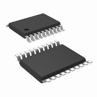
LM5035AMHX/NOPB National Semiconductor, LM5035AMHX/NOPB Datasheet - Page 26

LM5035AMHX/NOPB
Manufacturer Part Number
LM5035AMHX/NOPB
Description
IC PWM BCK BST FLYBK INV 20TSSOP
Manufacturer
National Semiconductor
Series
PowerWise®r
Datasheet
1.LM5035AMHNOPB.pdf
(30 pages)
Specifications of LM5035AMHX/NOPB
Pwm Type
Voltage Mode
Number Of Outputs
1
Frequency - Max
1MHz
Duty Cycle
92%
Voltage - Supply
13 V ~ 105 V
Buck
Yes
Boost
Yes
Flyback
Yes
Inverting
Yes
Doubler
No
Divider
No
Cuk
No
Isolated
Yes
Operating Temperature
-40°C ~ 125°C
Package / Case
20-TSSOP Exposed Pad, 20-eTSSOP, 20-HTSSOP
Frequency-max
1MHz
For Use With
LM5035AEVAL - BOARD EVAL FOR LM5035ALM5035EVAL - BOARD EVALUATION LM5035
Lead Free Status / RoHS Status
Lead free / RoHS Compliant
Other names
LM5035AMHX
Available stocks
Company
Part Number
Manufacturer
Quantity
Price
Company:
Part Number:
LM5035AMHX/NOPB
Manufacturer:
NS/TI
Quantity:
1 250
Part Number:
LM5035AMHX/NOPB
Manufacturer:
NS/国半
Quantity:
20 000
www.national.com
Printed Circuit Board Layout
The LM5035A Current Sense and PWM comparators are very
fast, and respond to short duration noise pulses. The compo-
nents at the CS, COMP, SS, OVP, UVLO, DLY and the RT
pins should be as physically close as possible to the IC, there-
by minimizing noise pickup on the PC board tracks.
Layout considerations are critical for the current sense filter.
If a current sense transformer is used, both leads of the trans-
former secondary should be routed to the sense filter com-
ponents and to the IC pins. The ground side of the transformer
should be connected via a dedicated PC board track to the
AGND pin, rather than through the ground plane.
If the current sense circuit employs a sense resistor in the
drive transistor source, low inductance resistors should be
used. In this case, all the noise sensitive, low-current ground
tracks should be connected in common near the IC, and then
a single connection made to the power ground (sense resistor
ground point).
The gate drive outputs of the LM5035A should have short,
direct paths to the power MOSFETs in order to minimize in-
ductance in the PC board traces. The SR control outputs
should also have minimum routing distance through the pulse
transformers and through the secondary gate drivers to the
sync FETs.
The two ground pins (AGND, PGND) must be connected to-
gether with a short, direct connection, to avoid jitter due to
relative ground bounce.
TABLE 2. Differences between LM5035, LM5035A, LM5035A-1, LM5035B, and
LM5035C
T1 = Delay from SR1, SR2 to leading edge of HO, LO
Performance Feature:
Sync Rectifier Dead-time Ratio
(T1:T2)
Soft-start: Hiccup Mode Charging
Current
Bootstrap (HB-HS) Under-Voltage
Lockout
Start-up Regulator Current
SR State in UVLO Shutdown and
Hiccup Current Limit
HO,LO On-Time at Max Duty Cycle 0.5*T-T1–70 ns
Soft-Stop after
UVLO
SR1, SR2 VOH (high state output)
Package
HO,LO
SR1,2
TSSOP20–EP
20mA (min)
50µA:1µA
LM5035
LLP24
VCC
High
Yes
Yes
2:1
5V
0.5*T-T1–70 ns
TSSOP20–EP
25mA (min)
100µA:1µA
LM5035A
LLP24
3.9V
High
VCC
Yes
Yes
3:1
26
If the internal dissipation of the LM5035A produces high junc-
tion temperatures during normal operation, the use of multiple
vias under the IC to a ground plane can help conduct heat
away from the IC. Judicious positioning of the PC board within
the end product, along with use of any available air flow
(forced or natural convection) will help reduce the junction
temperatures. If using forced air cooling, avoid placing the
LM5035A in the airflow shadow of tall components, such as
input capacitors.
Application Circuit Example
The following schematic shows an example of a 100W half-
bridge power converter controlled by the LM5035A. The op-
erating input voltage range (V
output voltage is 3.3V. The output current capability is 30
Amps. Current sense transformer T2 provides information to
the CS pin for current limit protection. The error amplifier and
reference, U3 and U5 respectively, provide voltage feedback
via opto-coupler U4. Synchronous rectifiers Q4, Q5, Q6 and
Q7 minimize rectification losses in the secondary. An auxiliary
winding on transformer T1 provides power to the LM5035A
VCC pin when the output is in regulation. The input voltage
UVLO thresholds are
for decreasing V
the ON/OFF input (J2) below 1.25V with an open-collector or
open-drain circuit. An external synchronizing frequency can
be applied through a 100pF capacitor to the RT input (U1 pin
5). The regulator output is current limited at
T
= Period of HO or LO
0.5*T-T1–70 ns
TSSOP28–EP
LM5035A-1
25mA (min)
100µA:1µA
3.9V
VCC
High
Yes
Yes
3:1
PWR
. The circuit can be shut down by driving
≊
34V for increasing V
TSSOP–20EP
40mA (min)
100µA:1µA
LM5035B
0.5*T-T1
LLP24
3.9V
VCC
Low
Yes
PWR
3:1
No
) is 36V to 75V, and the
≊
TSSOP20–EP
PWR
40mA (min)
34A.
100µA:1µA
LM5035C
REF (5V)
0.5*T-T1
LLP24
, and
3.9V
Low
3:1
No
No
≊
32V


