ISL6316CRZ Intersil, ISL6316CRZ Datasheet
ISL6316CRZ
Specifications of ISL6316CRZ


Related parts for ISL6316CRZ

ISL6316CRZ Summary of contents
Page 1
... ISL6316 with any other voltage rail. Dynamic-VID™ technology allows seamless on-the-fly VID changes. The offset pin allows accurate voltage offset settings that are independent of VID setting. Ordering Information PART NUMBER/ PART MARKING TEMP. (°C) PACKAGE ISL6316CRZ + 6x6 QFN (Note) (Pb-free) ISL6316IRZ* - 6x6 QFN (Note) (Pb-free) *Add “ ...
Page 2
Pinout NC VID5 VID4 VID3 VID2 VID1 VID0 GND OFS DAC 2 ISL6316 ISL6316 (40 LD QFN) TOP VIEW GND ...
Page 3
ISL6316CR Block Diagram VDIFF PGOOD RGND x1 VSEN OVP SOFT-START +175mV FAULT LOGIC SS OFFSET OFS REF DAC VID5 VID4 DYNAMIC VID3 VID D/A VID2 VID1 VID0 COMP FB IDROOP VR_HOT THERMAL MONITORING VR_FAN TM 3 ISL6316 CLOCK AND AND ...
Page 4
Typical Application - 4-Phase Buck Converter with r FB COMP REF IDROOP DAC VDIFF VSEN VCC RGND VTT EN_VTT PGOOD ISL6316 ISEN1+ ISEN1- PWM1 PWM2 VID5 ISEN2+ VID4 ISEN2- VID3 PWM3 ISEN3+ VID2 ISEN3- VID1 PWM4 VID0 ISEN4+ ISEN4- VR_FAN ...
Page 5
Typical Application - 4-Phase Buck Converter with r FB COMP REF IDROOP DAC VDIFF VSEN VCC RGND VTT EN_VTT PGOOD ISL6316 ISEN1+ ISEN1- PWM1 PWM2 VID5 ISEN2+ VID4 ISEN2- VID3 PWM3 ISEN3+ VID2 ISEN3- VID1 PWM4 VID0 ISEN4+ ISEN4- VR_FAN ...
Page 6
Typical Application - 4-Phase Buck Converter with DCR Sensing and External TCOMP FB COMP REF IDROOP DAC VDIFF VSEN VCC RGND VTT EN_VTT PGOOD ISL6316 ISEN1+ ISEN1- PWM1 PWM2 VID5 ISEN2+ VID4 ISEN2- VID3 PWM3 ISEN3+ VID2 ISEN3- VID1 PWM4 ...
Page 7
Typical Application - 4-Phase Buck Converter with DCR Sensing and Integrated TCOMP FB COMP REF IDROOP DAC VDIFF VSEN VCC RGND VTT EN_VTT PGOOD ISL6316 ISEN1+ ISEN1- PWM1 PWM2 VID5 ISEN2+ VID4 ISEN2- VID3 PWM3 ISEN3+ VID2 ISEN3- VID1 PWM4 ...
Page 8
... Operating Conditions Supply Voltage, VCC . . . . . . . . . . . . . . . . . . . . . . . . . . . . . +5V ±5% Ambient Temperature (ISL6316CRZ 0°C to +70°C Ambient Temperature (ISL6316IRZ .-40°C to +85°C CAUTION: Stress above those listed in “Absolute Maximum Ratings” may cause permanent damage to the device. This is a stress only rating and operation of the device at these or any other conditions above those indicated in the operational section of this specification is not implied ...
Page 9
... Electrical Specifications Operating Conditions: V PARAMETER PIN-ADJUSTABLE OFFSET Voltage at OFS Pin of ISL6316CRZ Voltage at OFS Pin of ISL6316IRZ OSCILLATORS Accuracy of Switching Frequency Setting Adjustment Range of Switching Frequency (Note 4) Soft-Start Ramp Rate Adjustment Range of Soft-Start Ramp Rate (Note 4) PWM GENERATOR Sawtooth Amplitude Max Duty Cycle ...
Page 10
Electrical Specifications Operating Conditions: V PARAMETER POWER GOOD AND PROTECTION MONITORS Leakage Current of PGOOD PGOOD Low Voltage Undervoltage Threshold PFGOOD Reset Voltage Overvoltage Protection Threshold Overvoltage Protection Reset Threshold NOTES: 3. These parts are designed and adjusted for accuracy ...
Page 11
... Dynamic VID™ operations. PWM1, PWM2, PWM3, PWM4 Pulse width modulation outputs. Connect these pins to the PWM input pins of the Intersil driver IC. The number of active channels is determined by the state of PWM3 and PWM4. Tie PWM3 to VCC to configure for 2-phase operation. Tie PWM4 to VCC to configure for 3-phase operation. ISEN1+, ISEN1- ...
Page 12
Interleaving The switching of each channel in a multiphase converter is timed to be symmetrically out of phase with each of the other channels 3-phase converter, each channel switches 1/3 cycle after the previous channel and 1/3 cycle ...
Page 13
PWM Operation The timing of each channel is set by the number of active channels. The default channel setting for the ISL6316 is four. The switching cycle is defined as the time between PWM pulse termination signals of each channel. ...
Page 14
ISL6605 INDUCTOR R PWM(n) ISL6316 INTERNAL CIRCUIT I n SAMPLE & ISEN-(n) HOLD + - ISEN+(n) DCR I I ----------------- - = SEN L R ISEN FIGURE 4. DCR SENSING CONFIGURATION With the internal low-offset current amplifier, ...
Page 15
... The output of the error amplifier, V COMP sawtooth waveform to generate the PWM signals. The PWM signals control the timing of the Intersil MOSFET drivers and regulate the converter output to the specified reference voltage. The internal and external circuitry which control voltage regulation is illustrated in Figure 8. ...
Page 16
TABLE 1. VR10 VID 6-BIT VID4 VID3 VID2 VID1 VID0 400mV 200mV 100mV 50mV 25mV ...
Page 17
As shown in Figure 8, a current proportional to the average current of all active channels, ...
Page 18
... ISL6316 that the driver ICs reach their POR level before the ISL6316 becomes enabled. The schematic in Figure 10 demonstrates sequencing the ISL6316 with the ISL66xx family of Intersil MOSFET drivers, which require 12V (EQ. 13) bias. 3. The voltage on EN_VTT must be higher than 0.875V to enable the controller. This pin is typically connected to the output of VTT VR ...
Page 19
... At the inception of an overvoltage event, all PWM outputs are commanded low instantly (less than 20ns) until the voltage at VDIFF falls below 0.4V. This causes the Intersil drivers to turn on the lower MOSFETs and pull the output voltage below a level that might cause damage to the load. The PWM outputs remain low until VDIFF falls below 0 ...
Page 20
... Accordingly, the reader is cautioned to verify that data sheets are current before placing orders. Information furnished by Intersil is believed to be accurate and reliable. However, no responsibility is assumed by Intersil or its subsidiaries for its use; nor for any infringements of patents or other rights of third parties which may result from its use ...
Page 21
VCC R 0.33V CC TM1 NTC 0.28V CC FIGURE 14. BLOCK DIAGRAM OF THERMAL MONITORING FUNCTION TEMPERATURE TM CC 100 ...
Page 22
When the TM NTC is placed close to the current sense component (inductor or MOSFET), the temperature of the NTC will track the temperature of the current sense component. Therefore the TM voltage can be utilized to obtain the temperature ...
Page 23
... It is assumed that the reader is familiar with many of the basic skills and techniques referenced below. In addition to this guide, Intersil provides complete reference designs that include schematics, bills of materials, and example board layouts for all common microprocessor applications. ...
Page 24
A third component involves the lower MOSFET’s reverse- recovery charge Since the inductor current has fully rr commutated to the upper MOSFET before the lower- MOSFET’s body diode can draw all of Q through the upper MOSFET across ...
Page 25
C (OPTIONAL COMP FB + IDROOP DROOP - VDIFF FIGURE 19. COMPENSATION CONFIGURATION FOR LOAD-LINE REGULATED ISL6316 CIRCUIT The feedback resistor has already been chosen as FB outlined in Load-Line ...
Page 26
In the solutions to the compensation equations, there is a single degree of freedom. For the solutions presented in Equation 33 selected arbitrarily. The remaining FB compensation components are then selected according to Equation 33 ...
Page 27
Input Supply Voltage Selection The VCC input of the ISL6316 can be connected either directly to a +5V supply or through a current limiting resistor to a +12V supply. An integrated 5.8V shunt regulator maintains the voltage on the VCC ...
Page 28
... The the components is minimized while creating the PHASE O plane. Place the Intersil MOSFET driver IC as close as possible to the MOSFETs they control to reduce the parasitic impedances due to trace length between critical driver input and output signals. If possible, duplicate the same placement of these components for each phase ...
Page 29
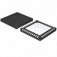
Package Outline Drawing L40.6x6 40 LEAD QUAD FLAT NO-LEAD PLASTIC PACKAGE Rev 3, 10/06 6.00 6 PIN 1 INDEX AREA (4X) 0.15 TOP VIEW ( TYP ) ( TYPICAL RECOMMENDED LAND PATTERN 29 ...