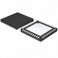
ISL6308ACRZ Intersil, ISL6308ACRZ Datasheet - Page 22

ISL6308ACRZ
Manufacturer Part Number
ISL6308ACRZ
Description
IC CTRLR PWM BUCK 3PHASE 40-QFN
Manufacturer
Intersil
Datasheet
1.ISL6308ACRZ-T.pdf
(28 pages)
Specifications of ISL6308ACRZ
Pwm Type
Voltage Mode
Number Of Outputs
1
Frequency - Max
275kHz
Duty Cycle
66.6%
Voltage - Supply
4.75 V ~ 5.25 V
Buck
Yes
Boost
No
Flyback
No
Inverting
No
Doubler
No
Divider
No
Cuk
No
Isolated
No
Operating Temperature
0°C ~ 70°C
Package / Case
40-VFQFN, 40-VFQFPN
Frequency-max
275kHz
Lead Free Status / RoHS Status
Lead free / RoHS Compliant
Available stocks
Company
Part Number
Manufacturer
Quantity
Price
Part Number:
ISL6308ACRZ
Manufacturer:
INTERSIL
Quantity:
20 000
Part Number:
ISL6308ACRZ-T
Manufacturer:
INTERSIL
Quantity:
20 000
In Equations 28, L is the per-channel filter inductance
divided by the number of active channels; C is the sum total
of all output capacitors; ESR is the equivalent series
resistance of the bulk output filter capacitance; and V
the peak-to-peak sawtooth signal amplitude, as described in
the “Electrical Specifications” table.
Once selected, the compensation values in Equations 28
assure a stable converter with reasonable transient
performance. In most cases, transient performance can be
improved by making adjustments to R
value of R
oscilloscope until no further improvement is noted. Normally,
C
Equations 28 unless some performance issue is noted.
The optional capacitor C
noise away from the PWM comparator (see Figure 19). Keep
a position available for C
frequency capacitor of between 22pF and 150pF in case any
leading edge jitter problem is noted.
Compensating the Converter Operating Without
Load-Line Regulation
The ISL6308A multi-phase converter operating without load
line regulation behaves in a similar manner to a voltage-
mode controller. This section highlights the design
consideration for a voltage-mode controller requiring external
compensation. To address a broad range of applications, a
type-3 feedback network is recommended (see Figure 20).
Figure 21 highlights the voltage-mode control loop for a
synchronous-rectified buck converter, applicable, with a
small number of adjustments, to the multi-phase ISL6308A
circuit. The output voltage (V
voltage, VREF, level. The error amplifier output (COMP pin
Case 3:
1
FIGURE 20. COMPENSATION CONFIGURATION FOR
will not need adjustment. Keep the value of C
C
R
3
2
3
while observing the transient performance on an
NON-LOAD-LINE REGULATED ISL6308A
F
R
C
0
2
2
>
=
=
R
-------------------------------- -
2π C ESR
R
1
R
-------------------------------------------------------------- -
2π V
2
0.66 V
1
⋅
2
2
⋅
, is sometimes needed to bypass
⋅
C
, and be prepared to install a high
1
2π F
-----------------------------------------------
⋅
2
0.66 V
OUT
OSC
⋅
C
22
⋅
1
IN
) is regulated to the reference
⋅
0
⋅
⋅
R
⋅
ESR
IN
V
1
COMP
OSC
VDIFF
⋅
⋅
F
FB
ESR
2
⋅
0
. Slowly increase the
⋅
⋅
C
L
L
ISL6308A
1
from
PP
is
ISL6308A
voltage) is compared with the oscillator (OSC) modified saw-
tooth wave to provide a pulse-width modulated wave with an
amplitude of V
smoothed by the output filter (L and C). The output filter
capacitor bank’s equivalent series resistance is represented by
the series resistor E.
The modulator transfer function is the small-signal transfer
function of V
gain, given by d
filter, with a double pole break frequency at F
F
the individual channel inductance and its DCR divided by 3
(equivalent parallel value of the three output inductors), while
C and ESR represents the total output capacitance and its
equivalent series resistance.
The compensation network consists of the error amplifier
(internal to the ISL6308A) and the external R
components. The goal of the compensation network is to
provide a closed loop transfer function with high 0dB crossing
frequency (F
F
CE
LC
FIGURE 21. VOLTAGE-MODE BUCK CONVERTER
=
. For the purpose of this analysis, L and DCR represent
CIRCUIT
PWM
---------------------------
2π
⋅
1
COMP
L C
OUT
0
⋅
; typically 0.1 to 0.3 of F
COMPENSATION DESIGN
IN
HALF-BRIDGE
MAX
at the PHASE node. The PWM wave is
OSCILLATOR
/V
V
COMP
OSC
E/A
DRIVE
V
R
ISL6308A
IN
2
/V
. This function is dominated by a DC
C
F
+
-
+
VREF
OSC
2
-
CE
C
=
1
, and shaped by the output
-------------------------------- -
2π C ESR
FB
PHASE
UGATE
LGATE
VDIFF
RGND
VSEN
EXTERNAL CIRCUIT
⋅
SW
1
⋅
R
3
V
) and adequate phase
IN
R
1
1
C
LC
-R
L
3
3
and a zero at
September 9, 2008
, C
DCR
V
ESR
1
(EQ. 29)
OUT
-C
C
3
FN6669.0


