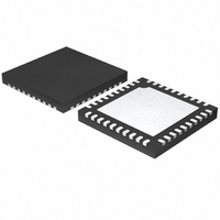
ISL6326CRZ-T Intersil, ISL6326CRZ-T Datasheet - Page 23

ISL6326CRZ-T
Manufacturer Part Number
ISL6326CRZ-T
Description
IC CTRLR PWM 4PHASE BUCK 40-QFN
Manufacturer
Intersil
Datasheet
1.ISL6326CRZ.pdf
(30 pages)
Specifications of ISL6326CRZ-T
Pwm Type
Voltage Mode
Number Of Outputs
1
Frequency - Max
275kHz
Duty Cycle
25%
Voltage - Supply
4.75 V ~ 5.25 V
Buck
Yes
Boost
No
Flyback
No
Inverting
No
Doubler
No
Divider
No
Cuk
No
Isolated
No
Operating Temperature
0°C ~ 70°C
Package / Case
40-VFQFN, 40-VFQFPN
Frequency-max
275kHz
Lead Free Status / RoHS Status
Lead free / RoHS Compliant
Available stocks
Company
Part Number
Manufacturer
Quantity
Price
Part Number:
ISL6326CRZ-T
Manufacturer:
INTERSIL
Quantity:
20 000
TCOMP voltage can also be used to compensate for the
difference between the recommended TM voltage curve in
Figure 13 and that of the actual design. According to the
VCC voltage, ISL6326 converts the TCOMP pin voltage to a
4-bit TCOMP digital signal as TCOMP factor N.
The TCOMP factor N is an integer between 0 and 15. The
integrated temperature compensation function is disabled for
N = 0. For N = 4, the NTC temperature is equal to the
temperature of the current sense component. For N < 4, the
NTC is hotter than the current sense component. The NTC is
cooler than the current sense component for N > 4. When
N > 4, the larger TCOMP factor N, the larger the difference
between the NTC temperature and the temperature of the
current sense component.
ISL6326 multiplexes the TCOMP factor N with the TM digital
signal to obtain the adjustment gain to compensate the
temperature impact on the sensed channel current. The
compensated channel current signal is used for droop and
overcurrent protection functions.
Design Procedure
10. Record the output voltage as V1 immediately after the
1. Properly choose the voltage divider for the TM pin to
2. Run the actual board under the full load and the desired
3. After the board reaches the thermal steady state, record
4. Use Equation 20 to calculate the resistance of the TM
5. Use Equation 21 to calculate the TCOMP factor N:
6. Choose an integral number close to the above result for
7. Choose the pull-up resistor R
8. If N = 15, do not need the pull-down resistor R
9. Run the actual board under full load again with the proper
match the TM voltage vs temperature curve with the
recommended curve in Figure 12.
cooling condition.
the temperature (T
(inductor or MOSFET) and the voltage at TM and VCC
pins.
NTC, and find out the corresponding NTC temperature
T
the TCOMP factor. If this factor is higher than 15, use
N = 15. If it is less than 1, use N = 1.
otherwise obtain R
resistors connected to the TCOMP pin.
output voltage is stable with the full load. Record the
output voltage as V2 after the VR reaches the thermal
steady state.
R
N
R
NTC
NTC T
TC2
=
209x T
------------------------------------------------------- -
(
from the NTC datasheet.
=
NTC
3xT
NxR
---------------------- -
(
15 N
NTC
)
CSC
–
TC1
=
V
------------------------------- -
V
+
–
TM
CC
400
T
CSC
TC2
NTC
xR
–
V
TM1
)
) of the current sense component
TM
by using Equation 22:
+
23
4
TC1
(typical 10kΩ).
TC2
(EQ. 20)
(EQ. 21)
(EQ. 22)
,
ISL6326
11. If the output voltage increases over 2mV as the
External Temperature Compensation
By pulling the TCOMP pin to GND, the integrated
temperature compensation function is disabled. And one
external temperature compensation network (shown in
Figure 15) can be used to cancel the temperature impact on
the droop (i.e. load line).
The sensed current will flow out of the IDROOP pin and
develop a droop voltage across the resistor equivalent (R
between the FB and VDIFF pins. If R
as the temperature increases, the temperature impact on the
droop can be compensated. An NTC resistor can be placed
close to the power stage and used to form R
non-linear temperature characteristics of the NTC, a resistor
network is needed to make the equivalent resistance
between the FB and VDIFF pins reverse proportional to the
temperature.
The external temperature compensation network can only
compensate the temperature impact on the droop, while it
has no impact to the sensed current inside ISL6326.
Therefore, this network cannot compensate for the
temperature impact on the overcurrent protection function.
Current Sense Output
The current from the IDROOP pin is the sensed average
current inside the ISL6326. In typical application, the
IDROOP pin is connected to the FB pin for the application
where load line is required.
When load line function is not needed, the IDROOP pin can
be used to obtain the load current information: with one
resistor from the IDROOP pin to GND, the voltage at the
IDROOP pin will be proportional to the load current in
Equation 23:
V
FIGURE 15. EXTERNAL TEMPERATURE COMPENSATION
IDROOP
temperature increases, i.e. V2 - V1 > 2mV, reduce N and
redesign R
as the temperature increases, i.e. V1 - V2 > 2mV,
increase N and redesign R
=
--------------------------- -
R
IDROOP
TC2
N
°C
; if the output voltage decreases over 2mV
----------------- - I
R
ISEN
R
X
IDROOP
COMP
VDIFF
LOAD
TC2
FB
.
FB
ISL6326
INTERNAL
CIRCUIT
resistance reduces
FB
. Due to the
May 5, 2008
(EQ. 23)
FN9262.1
FB
)


