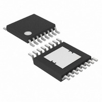
MAX15005AAUE+T Maxim Integrated Products, MAX15005AAUE+T Datasheet - Page 19

MAX15005AAUE+T
Manufacturer Part Number
MAX15005AAUE+T
Description
IC PWR SUPPLY CNTRLR 16-TSSOP
Manufacturer
Maxim Integrated Products
Datasheet
1.MAX15005BAUE.pdf
(27 pages)
Specifications of MAX15005AAUE+T
Pwm Type
Current Mode
Number Of Outputs
1
Frequency - Max
1MHz
Duty Cycle
81.5%
Voltage - Supply
4.5 V ~ 40 V
Buck
No
Boost
Yes
Flyback
Yes
Inverting
No
Doubler
No
Divider
Yes
Cuk
No
Isolated
Yes
Operating Temperature
-40°C ~ 125°C
Package / Case
16-TSSOP Exposed Pad, 16-eTSSOP, 16-HTSSOP
Frequency-max
1MHz
Duty Cycle (max)
80 %
Output Voltage
1.23 V to 100 V
Output Current
1000 mA
Mounting Style
SMD/SMT
Switching Frequency
15 KHz to 500 KHz
Maximum Operating Temperature
+ 125 C
Minimum Operating Temperature
- 40 C
Synchronous Pin
Yes
Topology
Boost, Flyback, Forward
Lead Free Status / RoHS Status
Lead free / RoHS Compliant
Step 3) Calculate the secondary to primary turns ratio
(N
using the following equations:
and
The forward bias drops of the secondary diode and the
bias rectifier diode are assumed to be 0.35V and 0.7V,
respectively. Refer to the diode manufacturer’s
datasheet to verify these numbers.
Step 4) The transformer manufacturer needs the RMS
current maximum values in the primary, secondary, and
bias windings to design the wire diameter for the differ-
ent windings. Use only wires with a diameter smaller
than 28AWG to keep skin effect losses under control.
To achieve the required copper cross-section, multiple
wires must be used in parallel. Multifilar windings are
common in high-frequency converters. Maximum RMS
currents in the primary and secondary occur at 50%
duty cycle (minimum input voltage) and maximum out-
put power. Use the following equations to calculate the
primary and secondary RMS currents:
The bias current for most MAX15004/MAX15005 applica-
tions is about 20mA and the selection of wire depends
more on convenience than on current capacity.
Step 5) The winding technique and the windings
sequence is important to reduce the leakage induc-
tance spike at switch turn-off. For example, interleave
the secondary between two primary halves. Keep the
bias winding close to the secondary, so that the bias
voltage tracks the output voltage.
MOSFET selection criteria include the maximum drain
voltage, peak/RMS current in the primary and the maxi-
mum-allowable power dissipation of the package with-
out exceeding the junction temperature limits. The
voltage seen by the MOSFET drain is the sum of the
input voltage, the reflected secondary voltage through
transformer turns ratio and the leakage inductance
SP
Flyback/Boost/SEPIC Power-Supply Controllers
) and the bias winding to primary turns ratio (N
I
I
PRMS
SRMS
=
=
N
0 5
0 0 5
BP
.
. × D
=
×
______________________________________________________________________________________
N
I
D
N
OUT
SP
MAX
OFFMAX
BIAS
N
P
=
P
OUT
N
N
×
P
S
=
η
V
=
×
OUT
V
D
INMIN
L
L
11 7
OFFMAX
P
S
MOSFET Selection
+
.
3
0 35
.
×
D
4.5V to 40V Input Automotive
MAX
3
BP
)
spike. The MOSFET’s absolute maximum V
must be higher than the worst-case (maximum input
voltage and output load) drain voltage.
Lower maximum V
channel, lower R
package. A lower N
specification and keeps the leakage inductance spike
under control. A resistor/diode/capacitor snubber net-
work can be also used to suppress the leakage induc-
tance spike.
The DC losses in the MOSFET can be calculated using
the value for the primary RMS maximum current.
Switching losses in the MOSFET depend on the operat-
ing frequency, total gate charge, and the transition loss
during turn-off. There are no transition losses during
turn-on since the primary current starts from zero in the
discontinuous conduction mode. MOSFET derating
may be necessary to avoid damage during system
turn-on and any other fault conditions. Use the following
equation to estimate the power dissipation due to the
power MOSFET:
where:
Q
V
t
C
The output capacitance requirements for the flyback
converter depend on the peak-to-peak ripple accept-
able at the load. The output capacitor supports the load
current during the switch on-time. During the off-cycle,
the transformer secondary discharges the core replen-
ishing the lost charge and simultaneously supplies the
load current. The output ripple is the sum of the voltage
drop due to charge loss during the switch on-time and
the ESR of the output capacitor. The high switching fre-
quency of the MAX15004/MAX15005 reduces the
capacitance requirement.
OFF
P
IN
DS
g
MOS
V
= Total gate charge of the MOSFET (C) at 7.4V
DSMAX
= Input voltage (V)
= Drain-to-source capacitance (F)
= Turn-off time (s)
=
( .
1 4
=
(
×
V
V
R
I I NMAX
INMAX
DSON
+
DS-ON
C
DS
DS
×
×
+
P
I
×
PK
/N
, lower gate charge, and smaller
I
⎡
⎢
⎢
⎣
2
requirement means a shorter
V
N
PRMS
N
DS
S
×
S
P
4
t
ratio allows a low V
2
2
OFF
×
×
) (
(
+
f
V
OUTMAX
×
OUT
Q
f
Output Filter Design
OUTMAX
g
×
+
V
V
IN
D
)
×
)
⎤
⎥
⎥
⎦
f
OUTMAX
+
DS
V
SPIKE
DSMAX
rating
)
19
+


