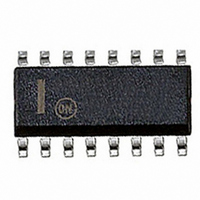
MC34025DWG ON Semiconductor, MC34025DWG Datasheet - Page 14

MC34025DWG
Manufacturer Part Number
MC34025DWG
Description
IC CTRLR PWM DBL END HF 16SOIC
Manufacturer
ON Semiconductor
Datasheet
1.MC34025DWR2G.pdf
(20 pages)
Specifications of MC34025DWG
Pwm Type
Voltage/Current Mode
Number Of Outputs
2
Frequency - Max
1MHz
Duty Cycle
45%
Voltage - Supply
10 V ~ 30 V
Buck
No
Boost
No
Flyback
No
Inverting
No
Doubler
No
Divider
No
Cuk
No
Isolated
Yes
Operating Temperature
0°C ~ 70°C
Package / Case
16-SOIC (0.300", 7.5mm Width)
Frequency-max
1MHz
Duty Cycle (max)
45 %
Output Voltage
5.05 V to 5.15 V
Output Current
500 mA
Mounting Style
SMD/SMT
Switching Frequency
1000 KHz
Operating Supply Voltage
30 V
Maximum Operating Temperature
+ 70 C
Fall Time
30 ns
Minimum Operating Temperature
0 C
Rise Time
30 ns
Synchronous Pin
Yes
Topology
Half-Bridge, Push-Pull
Lead Free Status / RoHS Status
Lead free / RoHS Compliant
Other names
MC34025DWGOS
Available stocks
Company
Part Number
Manufacturer
Quantity
Price
Part Number:
MC34025DWG
Manufacturer:
ON/安森美
Quantity:
20 000
The totem pole output can easily drive pulse transformers. A Schottky diode is recommended when driving inductive loads at high
frequencies. The diode can reduce the driver’s power dissipation due to excessive ringing, by preventing the output pin from being driven
below ground.
In current mode operation, this circuit will limit the maximum
voltage allowed at the ramp input to end a cycle.
In voltage mode operation, the maximum duty cycle can be
clamped. By the addition of a PNP transistor to buffer the clamp
voltage, the Soft−Start current is not affected by R
T
T
The new equation for Soft−Start is
Q
Q
Q
Q
Figure 32. Buffered Maximum Clamp Level
R
R
1
2
Figure 34. Isolated MOSFET Drive
V
ref
C
SS
1
2
8
t [
15
14
11
12
15
14
11
12
V
C
V clamp ) 0.6
V
C
Figure 36. MOSFET Parasitic Oscillations
9.0 μA
Boundary
Isolation
+
Sense Input
To Current
1
.
C
http://onsemi.com
SS
R
S
V
in
14
A series gate resistor may be needed to damp high frequency
parasitic oscillation caused by a MOSFET’s input capacitance
and any series wiring inductance in the gate−source circuit. The
series resistor will also decrease the MOSFET’s switching speed.
A Schottky diode can reduce the driver’s power dissipation due to
excessive ringing, by preventing the output pin from being driven
below ground. The Schottky diode also prevents substrate
injection when the output pin is driven below ground.
+
0
The totem pole output can furnish negative base current for
enhanced transistor turn−off, with the addition of the capacitor in
series with the base.
-
T
I
B
Q
Q
Figure 33. Bipolar Transistor Drive
Base Charge
T
Removal
Figure 35. Direct Transformer Drive
Q
Q
15
14
11
12
V
C
Sense Input
To Current
15
14
11
12
V
V
C
C
R
V
S
in


