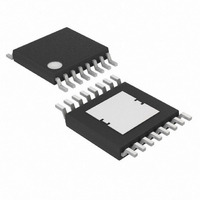
MAX5068AAUE+ Maxim Integrated Products, MAX5068AAUE+ Datasheet - Page 16

MAX5068AAUE+
Manufacturer Part Number
MAX5068AAUE+
Description
IC CNTRLR PWM CRNT MD 16TSSOP
Manufacturer
Maxim Integrated Products
Datasheet
1.MAX5068FAUE.pdf
(20 pages)
Specifications of MAX5068AAUE+
Pwm Type
Current Mode
Number Of Outputs
1
Frequency - Max
1.25MHz
Duty Cycle
50%
Voltage - Supply
10.8 V ~ 24 V
Buck
No
Boost
No
Flyback
Yes
Inverting
No
Doubler
No
Divider
No
Cuk
No
Isolated
Yes
Operating Temperature
-40°C ~ 125°C
Package / Case
16-TSSOP Exposed Pad, 16-eTSSOP, 16-HTSSOP
Frequency-max
1.25MHz
Duty Cycle (max)
50 %
Output Current
1000 mA
Mounting Style
SMD/SMT
Switching Frequency
25 KHz to 1250 KHz
Maximum Operating Temperature
+ 125 C
Minimum Operating Temperature
- 40 C
Synchronous Pin
Yes
Topology
Flyback, Forward
Lead Free Status / RoHS Status
Lead free / RoHS Compliant
optimally compensated, the current loop responds to
input-voltage transients within one cycle.
The current-sense resistor (R
the source of the MOSFET and ground, sets the current
limit. The CS input has a voltage trip level (V
314mV. Use the following equation to calculate the
value of R
where I
through the MOSFET at full load.
When the voltage produced by this current (through the
current-sense resistor) exceeds the current-limit com-
parator threshold, the MOSFET driver (NDRV) quickly
terminates the current on-cycle. In most cases, a small
RC filter is required to filter out the leading-edge spike
on the sense waveform. Set the corner frequency to a
few MHz above the switching frequency.
High-Frequency, Current-Mode PWM Controller
with Accurate Programmable Oscillator
16
______________________________________________________________________________________
PRI
CS
is the peak current in the primary that flows
:
R
CS
=
V
I
PRI
CS
CS
), connected between
Current Limit
CS
) of
Keep all PC board traces carrying switching currents
as short as possible, and minimize current loops.
For universal AC input design, follow all applicable safe-
ty regulations. Offline power supplies may require UL,
VDE, and other similar agency approvals. Contact these
agencies for the latest layout and component rules.
Typically, there are two sources of noise emission in a
switching power supply: high di/dt loops and high dv/dt
surfaces. For example, traces that carry the drain cur-
rent often form high di/dt loops. Similarly, the heatsink of
the MOSFET presents a dv/dt source, thus minimize the
surface area of the heatsink as much as possible.
To achieve best performance and to avoid ground
loops, use a solid ground-plane connection.
Applications Information
Layout Recommendations


