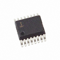
ISL6224CA Intersil, ISL6224CA Datasheet - Page 7

ISL6224CA
Manufacturer Part Number
ISL6224CA
Description
IC CONTROLLER PWM SINGLE 16-SSOP
Manufacturer
Intersil
Datasheet
1.ISL6224CAZ.pdf
(13 pages)
Specifications of ISL6224CA
Pwm Type
Current Mode
Number Of Outputs
1
Frequency - Max
690kHz
Duty Cycle
94%
Voltage - Supply
4 V ~ 24 V
Buck
Yes
Boost
No
Flyback
No
Inverting
No
Doubler
No
Divider
No
Cuk
No
Isolated
No
Operating Temperature
-10°C ~ 85°C
Package / Case
16-QSOP
Frequency-max
690kHz
Lead Free Status / RoHS Status
Contains lead / RoHS non-compliant
Available stocks
Company
Part Number
Manufacturer
Quantity
Price
Part Number:
ISL6224CA
Manufacturer:
INTERSIL
Quantity:
20 000
Part Number:
ISL6224CAZ
Manufacturer:
INTERSIL
Quantity:
20 000
Company:
Part Number:
ISL6224CAZ-T
Manufacturer:
INTERSIL
Quantity:
6 387
Operation-Mode Control
The mode-control circuit changes the converter’s mode of
operation based on the voltage polarity of the phase node
when the lower MOSFET is conducting and just before the
upper MOSFET turns on. For continuous inductor current,
the phase node is negative when the lower MOSFET is
conducting and the converters operate in fixed-frequency
PWM mode as shown in Figure 3. When the load current
decreases to the point where the inductor current flows
through the lower MOSFET in the ‘reverse’ direction, the
phase node becomes positive, and the mode is changed to
hysteretic.
A phase comparator handles the timing of the phase node
voltage sensing. A low level on the phase comparator output
indicates a negative phase voltage during the conduction
time of the lower MOSFET. A high level on the phase
comparator output indicates a positive phase voltage.
When the phase node is positive (phase comparator high),
at the end of the lower MOSFET conduction time, for eight
consecutive clock cycles, the mode is changed to hysteretic
as shown in Figure 3. The dashed lines indicate when the
phase node goes positive and the phase comparator output
goes high. The solid vertical lines at 1,2,...8 indicate the
sampling time, of the phase comparator, to determine the
polarity (sign) of the phase node. At the transition between
PWM and hysteretic mode both the upper and lower
MOSFETs are turned off. The phase node will ‘ring’ based
on the output inductor and the parasitic capacitance on the
phase node and settle out at the value of the output voltage.
The mode change from hysteretic to PWM can be caused by
one of two events. One event is the same mechanism that
causes a PWM to hysteretic transition. But instead of looking
for eight consecutive positive occurrences on the phase
node, it is looking for eight consecutive negative
occurrences on the phase node. The operation mode will be
changed from hysteretic to PWM when these eight
consecutive pulses occur. This transition technique prevents
jitter of the operation mode at load levels close to boundary.
The other mechanism for changing from hysteretic to PWM
is due to a sudden increase in the output current. This step
load causes an instantaneous decrease in the output voltage
PHASE
COMP
MODE
OF
OPERATION
VOUT
I
L
FIGURE 2. HYSTERETIC OPERATION MODE
1 2 3 4 5 6 7 8
PWM
7
HYSTERETIC
t
t
t
t
ISL6224
due to the voltage drop on the output capacitor ESR. If the
decrease causes the output voltage to drop below the
hysteretic regulation level, the mode is changed to PWM on
the next clock cycle. This insures the full power required by
the increase in output current.
Gate Control Logic
The gate control logic translates generated PWM control
signals into the MOSFET gate drive signals providing
necessary amplification, level shifting and shoot-through
protection. Also, it has functions that help optimize the IC
performance over a wide range of operational conditions.
Since MOSFET switching time can vary dramatically from
type to type and with the input voltage, the gate control logic
provides adaptive dead time by monitoring the gate-to-
source voltages of both upper and lower MOSFETs. The
lower MOSFET is not turned on until the gate-to-source
voltage of the upper MOSFET has decreased to less than
approximately 1V. Similarly, the upper MOSFET is not turned
on until the gate-to-source voltage of the lower MOSFET has
decreased to less than approximately 1V. This allows a wide
variety of upper and lower MOSFETs to be used without a
concern for simultaneous conduction, or shoot-through.
PHASE
NODE
I
PHASE
COMP
MODE
OF
OPERATION
L
FIGURE 3. MODE CONTROL WAVEFORMS
1
2
3
PWM
4
5
6
7
8
HYSTERETIC
June 8, 2006
FN9042.8
t
t
t
t


