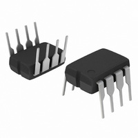
UC3843BNG ON Semiconductor, UC3843BNG Datasheet - Page 8

UC3843BNG
Manufacturer Part Number
UC3843BNG
Description
IC CTLR CURRENT MODE 8-DIP
Manufacturer
ON Semiconductor
Specifications of UC3843BNG
Pwm Type
Current Mode
Number Of Outputs
1
Frequency - Max
275kHz
Duty Cycle
96%
Voltage - Supply
8.2 V ~ 25 V
Buck
No
Boost
Yes
Flyback
Yes
Inverting
No
Doubler
No
Divider
No
Cuk
No
Isolated
Yes
Operating Temperature
0°C ~ 70°C
Package / Case
8-DIP (0.300", 7.62mm)
Frequency-max
275kHz
Duty Cycle (max)
96 % (Typ)
Output Voltage
4.9 V to 5.1 V
Output Current
1000 mA (Max)
Mounting Style
Through Hole
Switching Frequency
500 KHz
Operating Supply Voltage
30 V
Maximum Operating Temperature
70 C
Fall Time
50 ns
Minimum Operating Temperature
0 C
Rise Time
50 ns
Synchronous Pin
No
Topology
Boost or Flyback or Forward
Number Of Pwm Outputs
1
On/off Pin
No
Adjustable Output
No
Switching Freq
500kHz
Operating Supply Voltage (max)
30V
Operating Temperature Classification
Commercial
Mounting
Through Hole
Pin Count
8
Package Type
PDIP
Lead Free Status / RoHS Status
Lead free / RoHS Compliant
Other names
UC3843BNGOS
Available stocks
Company
Part Number
Manufacturer
Quantity
Price
Company:
Part Number:
UC3843BNG
Manufacturer:
ON
Quantity:
11 000
Company:
Part Number:
UC3843BNG
Manufacturer:
ON Semiconductor
Quantity:
3 300
Part Number:
UC3843BNG
Manufacturer:
ON/安森美
Quantity:
20 000
Part Number:
UC3843BNG ON
Manufacturer:
ON/安森美
Quantity:
20 000
fixed frequency, current mode controllers. They are
specifically designed for Off−Line and DC−to−DC
converter applications offering the designer a cost−effective
solution
representative block diagram is shown in Figure 19.
Oscillator
chosen for the timing components R
noted that the value of R
maximum duty ratio of UC384xx. The oscillator
configuration depicting the connection of the timing
components to the R
Figure 18. Capacitor C
through resistor R
typically 2.8 V. Upon reaching this peak threshold volage, an
internal 8.3 mA current source, I
voltage across C
across C
typically 1.2 V, I
charge up again from V
resulting waveform on the R
Typical waveforms are shown in Figure 20.
within ±6% at 50 kHz
trend of operating switching controllers at higher
frequencies, the UC384xx is guaranteed to operate within
±10% at 250 kHz
minimize variations of oscillator frequency and maximum
duty ratio.
capacitor C
equations do not take into account the propagation delays of
the internal comparator. Hence, at higher frequencies, the
calculated value of the oscillator frequency differs from the
actual value.
t
algebraic simplification, we obtain
RT CT(dischg)
The UC3842B, UC3843B series are high performance,
The oscillator frequency is programmed by the values
The oscillator thresholds are temperature compensated to
The charging and discharging times of the timing
The maximum duty ratio, D
Substituting Equations 1 and 2 into Equation 3, and after
t
RT CT(chg)
T
with
T
+ R
reaches its valley threshold, V
are calculated using Equations 1 and 2. These
D
+ R
max
T
dischg
C
T
T
minimal
T
+
T
C
begins to decrease. Once the voltage
ln
.
T
T
t
/C
to its peak threshold V
turns off. This allows capacitor C
ln
These internal circuit refinements
RT CT(chg)
T
ref
.
R
R
T
gets charged from the V
Considering the general industry
T
. This entire cycle repeats, and the
T
V
I
pin of the controller is shown in
V
I
dischg
dischg
RT CT(valley)
RT CT(peak)
T
t
/C
RT CT(chg)
T
external
max
) t
) V
T
) V
uniquely determines the
dischg
pin has a sawtooth shape.
is given by Equation 3.
RT CT(dischg)
T
RT CT(valley)
RT CT(peak)
and C
* V
* V
, is enabled and the
components.
ref
ref
T.
It must also be
OPERATING DESCRIPTION
* V
RT/CT(valley)
* V
RT/CT(peak)
ref
ref
ref
source,
(eq. 1)
(eq. 2)
(eq. 3)
http://onsemi.com
T
to
A
,
,
8
D
timing resistor R
achieve a desired maximum duty ratio. Once R
selected, C
switching frequency as per Equation 5.
f +
variation versus R
taken to ensure that the absolute minimum value of R
should not be less than 542 W. However, considering a 10%
tolerance for the timing resistor, the nearest available
standard resistor of 680 W is the absolute minimum that can
be used to guarantee normal oscillator operation. If a timing
resistor smaller than this value is used, then the charging
current through the R
(discharge) current and the oscillator will get permanently
locked/latched to an undefined state.
to frequency-lock the converter to an external system clock.
This can be accomplished by applying a clock signal to the
circuit shown in Figure 22. For reliable synchronization, the
free-running oscillator frequency should be set about 10%
less than the clock frequency. A method for multi-unit
synchronization is shown in Figure 23. By tailoring the
clock waveform, accurate Output duty ratio clamping can be
achieved.
max
Clearly, the maximum duty ratio is determined by the
Figure 2 shows the frequency and maximum duty ratio
In many noise-sensitive applications it may be desirable
R
+
T
C
ln
T
ln
Figure 18. Oscillator Configuration
V
V
T
RT CT(valley)
RT CT(peak)
V
V
Enable
can now be chosen to obtain the desired
RT CT(valley)
RT CT(peak)
T
T
. Therefore, R
for given values of C
ln
*V
T
*V
, C
*V
*V
V
ref
V
ref
I
RT CT(valley)
dischg
RT CT(peak)
T
ref
ref
@
path will exceed the pulldown
@
R T I dischg )V
R
1
T
R T I dischg )V
R
I
R
dischg
T
V
I
T
dischg
ref
/C
T
*V
*V
T
)V
is chosen such as to
ref
ref
)V
RT CT(valley)
C
RT CT(peak)
R
T
RT CT(valley)
T
RT CT(peak)
T
. Care should be
2.8 V
1.2 V
*V
*V
T
*V
*V
has been
ref
ref
ref
(eq. 4)
ref
(eq. 5)
T


