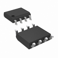
LP2996M/NOPB National Semiconductor, LP2996M/NOPB Datasheet - Page 10

LP2996M/NOPB
Manufacturer Part Number
LP2996M/NOPB
Description
IC DDR TERMINATION REG 8SOIC
Manufacturer
National Semiconductor
Datasheet
1.LP2996MNOPB.pdf
(18 pages)
Specifications of LP2996M/NOPB
Applications
Converter, DDR
Voltage - Input
2.2 ~ 5.5 V
Number Of Outputs
1
Operating Temperature
0°C ~ 125°C
Mounting Type
Surface Mount
Package / Case
8-SOIC (3.9mm Width)
Polarity
Positive
Input Voltage Max
5.5 V
Output Voltage
1.159 V, 1.259 V, 1.359 V
Output Type
Fixed
Output Current
1.5 A
Maximum Operating Temperature
+ 125 C
Mounting Style
SMD/SMT
Minimum Operating Temperature
0 C
Reference Voltage
1.358 V
Primary Input Voltage
2.5V
No. Of Outputs
1
No. Of Pins
8
Operating Temperature Range
0°C To +125°C
Msl
MSL 1 - Unlimited
Filter Terminals
SMD
Rohs Compliant
Yes
For Use With
LP2996MREVAL - BOARD EVALUATION LP2996MR
Lead Free Status / RoHS Status
Lead free / RoHS Compliant
Voltage - Output
-
Lead Free Status / Rohs Status
Details
Other names
*LP2996M
*LP2996M/NOPB
LP2996M
*LP2996M/NOPB
LP2996M
www.national.com
where a θ
for this calculation is 0.036 mm for 1oz. Copper.
FIGURE 3. LLP-16 θ
Additional improvements in lowering the θ
achieved with a constant airflow across the package. Main-
taining the same conditions as above and utilizing the 2x2 via
array,
FIGURE 4. θ
Figure 4
JA
of 50.41°C/W can be obtained. Via wall thickness
JA
shows how the θ
vs Airflow Speed (JEDEC Board with 4
JA
vs # of Vias (4 Layer JEDEC Board))
Vias)
JA
varies with airflow.
JA
can also be
20057508
20057509
10
Optimizing the θ
board exposed to lower ambient temperature allows the part
to operate with higher power dissipation. The internal power
dissipation can be calculated by summing the three main
sources of loss: output current at V
ing, and quiescent current at AVIN and VDDQ. During the
active state (when shutdown is not held low) the total internal
power dissipation can be calculated from the following equa-
tions:
Where,
To calculate the maximum power dissipation at V
ditions at V
current. Although only one equation will add into the total,
V
The power dissipation of the LP2996 can also be calculated
during the shutdown state. During this condition the output
V
disappear as it cannot sink or source any current (leakage is
negligible). The only losses during shutdown will be the re-
duced quiescent current at AVIN and the constant impedance
that is seen at the VDDQ pin.
TT
TT
cannot source and sink current simultaneously.
will tri-state, therefore that term in the power equation will
P
P
P
VDDQ
VDDQ
TT
VTT
P
need to be examined, sinking and sourcing
VTT
= ( V
JA
= V
= V
P
D
and placing the LP2996 in a section of a
= V
VDDQ
VDDQ
= P
P
P
P
PVIN
AVIN
AVIN
D
VTT
AVIN
= P
- V
* I
* I
= I
= I
x I
AVIN
VDDQ
VDDQ
VTT
+ P
AVIN
AVIN
LOAD
) x I
VDDQ
+ P
= V
= V
x V
* V
(Sinking) or
TT
LOAD
VDDQ
AVIN
VDDQ2
VDDQ2
, either sinking or sourc-
AVIN
+ P
(Sourcing
VTT
x R
x R
VDDQ
VDDQ
TT
both con-


