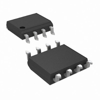
LP2996M/NOPB National Semiconductor, LP2996M/NOPB Datasheet - Page 11

LP2996M/NOPB
Manufacturer Part Number
LP2996M/NOPB
Description
IC DDR TERMINATION REG 8SOIC
Manufacturer
National Semiconductor
Datasheet
1.LP2996MNOPB.pdf
(18 pages)
Specifications of LP2996M/NOPB
Applications
Converter, DDR
Voltage - Input
2.2 ~ 5.5 V
Number Of Outputs
1
Operating Temperature
0°C ~ 125°C
Mounting Type
Surface Mount
Package / Case
8-SOIC (3.9mm Width)
Polarity
Positive
Input Voltage Max
5.5 V
Output Voltage
1.159 V, 1.259 V, 1.359 V
Output Type
Fixed
Output Current
1.5 A
Maximum Operating Temperature
+ 125 C
Mounting Style
SMD/SMT
Minimum Operating Temperature
0 C
Reference Voltage
1.358 V
Primary Input Voltage
2.5V
No. Of Outputs
1
No. Of Pins
8
Operating Temperature Range
0°C To +125°C
Msl
MSL 1 - Unlimited
Filter Terminals
SMD
Rohs Compliant
Yes
For Use With
LP2996MREVAL - BOARD EVALUATION LP2996MR
Lead Free Status / RoHS Status
Lead free / RoHS Compliant
Voltage - Output
-
Lead Free Status / Rohs Status
Details
Other names
*LP2996M
*LP2996M/NOPB
LP2996M
*LP2996M/NOPB
LP2996M
Typical Application Circuits
Several different application circuits have been shown in
ure 5
are possible in configuring the LP2996. Graphs of the indi-
vidual circuit performance can be found in the Typical Perfor-
mance Characteristics section in the beginning of the
datasheet. These curves illustrate how the maximum output
current is affected by changes in AVIN and PVIN.
If power dissipation or efficiency is a major concern then the
LP2996 has the ability to operate on split power rails. The
output stage (PVIN) can be operated on a lower rail such as
1.8V and the analog circuitry (AVIN) can be connected to a
higher rail such as 2.5V, 3.3V or 5V. This allows the internal
power dissipation to be lowered when sourcing current from
The third option for SSTL-2 applications in the situation that
a 1.8V rail is not available and it is not desirable to use 2.5V,
is to connect the LP2996 power rail to 3.3V. In this situation
AVIN will be limited to operation on the 3.3V or 5V rail as PVIN
can never exceed AVIN. This configuration has the ability to
provide the maximum continuous output current at the down-
through
Figure 14
to illustrate some of the options that
FIGURE 6. Lower Power Dissipation SSTL-2 Implementation
FIGURE 5. Recommended SSTL-2 Implementation
Fig-
11
SSTL-2 APPLICATIONS
For the majority of applications that implement the SSTL-2
termination scheme it is recommended to connect all the input
rails to the 2.5V rail. This provides an optimal trade-off be-
tween power dissipation and component count and selection.
An example of this circuit can be seen in
V
continuous current is reduced because of the lower rail volt-
age, although it is adequate for all motherboard SSTL-2 ap-
plications. Increasing the output capacitance can also help if
periods of large load transients will be encountered.
side of higher thermal dissipation. Care should be taken to
prevent the LP2996 from experiencing large current levels
which cause the junction temperature to exceed the maxi-
mum. Because of this risk it is not recommended to supply
the output stage with a voltage higher than a nominal 3.3V
rail.
TT
. The disadvantage of this circuit is that the maximum
20057510
20057511
Figure
5.
www.national.com


