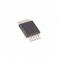
MAX5008CUB+ Maxim Integrated Products, MAX5008CUB+ Datasheet - Page 2

MAX5008CUB+
Manufacturer Part Number
MAX5008CUB+
Description
IC CHARGE PUMP USB 5V 10-UMAX
Manufacturer
Maxim Integrated Products
Datasheet
1.MAX5008CUB.pdf
(7 pages)
Specifications of MAX5008CUB+
Applications
Converter, USB
Voltage - Input
2.95 ~ 5.5 V
Number Of Outputs
1
Voltage - Output
5V
Operating Temperature
0°C ~ 70°C
Mounting Type
Surface Mount
Package / Case
10-MSOP, Micro10™, 10-uMAX, 10-uSOP
Function
Step Up, Step Down
Output Voltage
5 V
Output Current
140 mA
Maximum Operating Temperature
+ 70 C
Minimum Operating Temperature
0 C
Mounting Style
SMD/SMT
Lead Free Status / RoHS Status
Lead free / RoHS Compliant
ABSOLUTE MAXIMUM RATINGS
IN, SHDN, RCS, FAULT, OUT to GND .....................-0.3V to +6V
PGND to GND.....................................................................±0.3V
CXN to GND ................................................-0.3V to (V
CXP to GND ............................................-0.3V to (V
CEXT to GND ..........................................-0.3V to (V
Short-Circuit Duration to GND .......................................Indefinite
ELECTRICAL CHARACTERISTICS
(V
Typical values are at T
Regulated 5V USB Charge Pump with
Programmable Current Limit
2
Stresses beyond those listed under “Absolute Maximum Ratings” may cause permanent damage to the device. These are stress ratings only, and functional
operation of the device at these or any other conditions beyond those indicated in the operational sections of the specifications is not implied. Exposure to
absolute maximum rating conditions for extended periods may affect device reliability.
Input Voltage Range
(Note 1)
Input Undervoltage Lockout
Threshold
Input Undervoltage Lockout
Hysteresis
Output Voltage
(Note 2)
Output Voltage Ripple
V
Maximum Output Current
No-Load Input Current
SHDN Logic High
SHDN Logic Low
Shutdown Supply Current
Current-Sense Trip Level
FAULT Leakage Current
FAULT Logic Low
FAULT Assertion Delay
(Note 4)
FAULT Deassertion Delay (Note 5)
Switching Frequency
Startup Time
IN
OUT
_______________________________________________________________________________________
= SHDN = 3V, C
Fault Threshold
PARAMETER
IN
A
= 4.7µF, C
= +25°C.)
X
= 0.68µF, C
V
V
SYMBOL
INH,SHDN
INL,SHDN
I
t
QSHDN
V
START
I
t
V
V
V
V
OUT
FDD
t
OUT
I
RIP
FD
TH
CS
Q
IN
EXT
I
I
Rising edge
Falling edge
0
0mA
0mA
V
V
I
I
SHDN = low
V
V
I
I
V
I
V
of SHDN
CEXT
CEXT
OUT
OUT
OUT
OUT
OUT
OUT
OUT
OUT
OUT
CS
FAULT
OUT
OUT
= 6.8µF, C
IN
I
OUT
= I
= 125mA, 4.75V
= 70mA
= 0, V
= 0, V
> I
< I
> I
+ 0.3V)
+ 0.3V)
+ 0.3V)
= 5V 4%
= 5V (nominal), no load
< V
> V
I
I
OUT
OUT
OUT
LIMIT
LIMIT
LIMIT
= 5V, OUT in regulation
< 30mA, 2.95V < V
TH
TH
IN
IN
x R
, R
, or V
OUT
and V
= 4.25V
= 3.3V
125mA, 2.95V
125mA
LOAD
CS
CONDITIONS
= 4.7µF, R
OUT
(Note 3)
OUT
Continuous Power Dissipation (T
Operating Temperature Range...............................0°C to +70°C
Junction Temperature ......................................................+150°C
Storage Temperature Range .............................-65°C to +150°C
Lead Temperature (soldering, 10s) .................................+300°C
= 46 , from rising edge
10-Pin µMAX.................................................................444mW
< V
V
> 4.5V
OUT
TH
IN
CS
, I
< 5.5V
FAULT
V
= 0.4 , T
5.25V
IN
4.25V
= 1mA
A
= 0°C to +70°C, unless otherwise noted.
2.95
2.95
4.75
4.75
82.5
MIN
100
2.0
2.4
0.5
55
A
= +70°C)
TYP
2.35
100
100
140
200
5.0
5.0
0.6
0.1
60
30
16
1
2
1
MAX
4.25
5.50
5.30
5.25
92.5
2.6
0.4
0.4
1.5
10
73
6
6
1
%V
UNITS
MHz
mV
mV
mA
mA
mV
ms
ms
µA
µA
µs
µs
V
V
V
V
V
V
OUT


