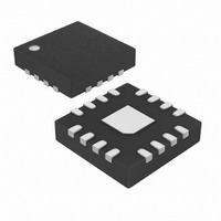
MAX15031ATE+ Maxim Integrated Products, MAX15031ATE+ Datasheet - Page 12

MAX15031ATE+
Manufacturer Part Number
MAX15031ATE+
Description
IC BOOST CONV/CURRENT MON 16TQFN
Manufacturer
Maxim Integrated Products
Datasheet
1.MAX15031ATE.pdf
(17 pages)
Specifications of MAX15031ATE+
Applications
Converter Current Monitor, APD Bias Applications
Voltage - Input
2.7 ~ 11 V
Number Of Outputs
1
Voltage - Output
3.7 ~ 76 V
Operating Temperature
-40°C ~ 125°C
Mounting Type
Surface Mount
Package / Case
16-TQFN Exposed Pad
Lead Free Status / RoHS Status
Lead free / RoHS Compliant
80V, 300mW Boost Converter and Current
Monitor for APD Bias Applications
Figure 1. Adjustable Output Voltage
Set the MAX15031 output voltage by connecting a resis-
tive divider from the output to FB to SGND (Figure 1).
Select R
400kΩ. Calculate R
lowing equation:
where V
= 1.245V or V
For V
voltage is used as the feedback set point (V
1.245V) and for V
If the boost converter remains in the discontinuous
mode of operation, then the approximate peak inductor
current, I
mula below:
where T
V
mum input voltage in volts, I
12
OUT
I
LPEAK
______________________________________________________________________________________
CNTRL
is the output voltage in volts, V
OUT
1
S
LPEAK
Determining Peak Inductor Current
=
(FB to SGND resistor) between 200kΩ and
is the switching period in microseconds,
> 1.5V, the internal 1.245V (typ) reference
can range from (V
2 T
CNTRL
×
(in amperes), is represented by the for-
MAX15031
CNTRL
R
S
2
2
×
=
Setting the Output Voltage
(V
depending on the V
(V
R
OUT
OUT
1
< 1.25V, V
⎡
⎢
⎢
⎣
⎛
⎝ ⎜
FB
Design Procedure
V
V
to FB resistor) using the fol-
−
OUT
REF
OUT_MAX
V
η
IN_MIN
IN
×
⎞
⎠ ⎟
L
+ 1V) to 76V and V
−
REF
1
⎤
⎥
⎥
⎦
) I
IN_MIN
R
R
×
2
1
= V
is the maximum
OUT_MAX
V
CNTRL
CNTRL
OUT
is the mini-
.
REF
value.
REF
=
output current in amperes, L is the inductor value in
microhenrys, and η is the efficiency of the boost con-
verter (see the Typical Operating Characteristics ).
Three key inductor parameters must be specified for
operation with the MAX15031: inductance value (L),
inductor saturation current (I
(DCR). In general, the inductor should have a saturation
current rating greater than the maximum switch peak
current-limit value (I
with a low-DCR resistance for reasonable efficiency.
Use the following formula to calculate the lower bound
of the inductor value at different output voltages and
output currents. This is the minimum inductance value
for discontinuous mode operation for supplying full
300mW of output power.
where V
amperes) are typical values (so that efficiency is opti-
mum for typical conditions), T
period, η is the efficiency, and I
switch current in amperes (see the Electrical
Characteristics table).
Calculate the optimum value of L (L
the full output power without reaching the boundary
between continuous conduction mode (CCM) and DCM
using the following formula:
For a design in which V
3mA, η = 45%, I
1.3μH and L
For a worse-case scenario in which V
70V, I
2.5μs: L
The choice of 4.7μH is reasonable given the worst-case
scenario above. In general, the higher the inductance,
the lower the switching noise. Load regulation is also
better with higher inductance.
where L
OUT
L
MIN
MIN
MAX
IN_MIN
= 4mA, η = 43%, I
[ H]
μ
= 1.8μH and L
MAX
[ H]
μ
L
Determining the Inductor Value
OPTIMUM
=
, V
LIM_LX
=
= 23μH.
2 T
V
OUT
×
LIM_LX
IN_MIN
2
S
= 1.3A, and T
[ H]
×
IN
(both in volts), and I
μ
I
OUT
(V
MAX
2
= 1.6A). Choose an inductor
= 3.3V, V
η
OUT
× ×
=
×
S
SAT
I
L
OUT
LIM_LX
×
I
= 15μH.
LIM_LX
2
(in microseconds) is the
MAX
(V
−
2 25
), and DC resistance
OUT
V
.
IN_MIN
×
LIM_LX
OPTIMUM
[
μ
V
OUT
= 1.3A, and T
IN
S
H
OUT
2
−
]
= 2.5μs: L
V
= 2.9V, V
IN_MIN
) T
= 70V, I
×
is the peak
) to ensure
S
×
)
OUT
η
OUT
MIN
OUT
S
(in
=
=
=
=


