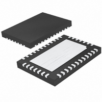
LT3513EUHF#TRPBF Linear Technology, LT3513EUHF#TRPBF Datasheet - Page 11

LT3513EUHF#TRPBF
Manufacturer Part Number
LT3513EUHF#TRPBF
Description
IC REG 5-OUT FOR TFT-LCD 38QFN
Manufacturer
Linear Technology
Datasheet
1.LT3513EUHFPBF.pdf
(22 pages)
Specifications of LT3513EUHF#TRPBF
Applications
Converter, TFT, LCD
Voltage - Input
4.5 ~ 30 V
Number Of Outputs
5
Voltage - Output
0.8 ~ 40 V
Operating Temperature
-40°C ~ 125°C
Mounting Type
Surface Mount
Package / Case
38-QFN
Lead Free Status / RoHS Status
Lead free / RoHS Compliant
Available stocks
Company
Part Number
Manufacturer
Quantity
Price
operaTion
The LT3513 is a highly integrated power supply IC contain-
ing four separate switching regulators and a low dropout
linear regulator (LDO). Switching regulator 1 is a step-
down 2.2A regulator with inductor current sense and an
integrated boost Schottky diode. Switching regulator 2 can
be configured as a step-up or SEPIC converter and has a
1.5A switch. Switching regulator 3 consists of a step-up
regulator with a 0.25A switch as well as an integrated
Schottky diode. Switching regulator 4 is a negative regula-
tor with a switch current limit of 0.25A and an integrated
Schottky diode. Linear regulator 5 is capable of providing
8mA of current to the base of an external NPN transistor.
The regulators share common circuitry including input
source, voltage reference and master oscillator. Operation
can be best understood by referring to the Block Diagram
as shown in Figure 1.
If the RUN-SS1 pin is pulled to ground, the LT3513 is shut
down and draws 30µA from the input source tied to V
An internal 2µA current source charges the external soft-
start capacitor, generating a voltage ramp at this pin. If the
RUN-SS1 pin exceeds 0.8V, the internal bias circuits turn
on, including the internal regulator, reference and 2MHz
master oscillator. The master oscillator generates four
clock signals, one for each of the switching regulators.
Switching regulator 1 will only begin to operate when the
RUN-SS1 pin reaches 0.8V. Switcher 1 generates V
which must be tied to the BIAS pin. When BIAS reaches 2.8V,
the NPNs pulling down on the RUN-SS2 and RUN-SS3/4
pins turns off, allowing an internal 2µA current source
to charge the external capacitors tied to RUN-SS2 and
RUN-SS3/4 pins. When the voltage on RUN-SS2 reaches
0.8V, switcher 2 is enabled. Correspondingly, when the
voltage on RUN-SS3/4 reaches 0.8V, switchers 3 and 4
are enabled. AV
rate determined by the capacitors tied to the RUN-SS2 and
RUN-SS3/4 pins. When all four switching outputs reach
90% of their programmed voltages, the NPN pulling down
DD
, E3 and V
OFF
will then begin rising at a
LOGIC
IN
.
,
on the C
source will charge the external capacitor tied to the C
When the C
turns on, connecting V
four outputs dropping below 90% of their programmed
voltage, PanelProtect circuitry pulls the C
disabling V
Figure 2. LT3513 Power-Up Sequence. (Traces from Both Photos
are Synchnonized to the Same Trigger)
PGOOD 20V/DIV
RUN-SS 2V/DIV
I
I
SS-234 2V/DIV
L4
L3
V
V
I
AV
V
L2
SS3/4
V
LOGIC
V
OFF
500mA/DIV
500mA/DIV
ON
V
E3
DD
500µA/DIV
I
CT
L1
10V/DIV
20V/DIV
20V/DIV
10V/DIV
2V/DIV
2V/DIV
5V/DIV
1A/DIV
T
pin will turn off, and an internal 20µA current
ON
T
pin reaches 1.1V, the output disconnect PNP
.
ON
to E3. In the event of any of the
(2a)
(2b)
5ms/DIV
5ms/DIV
T
LT3513
pin to GND,
11
3513 F02b
3513 F02a
T
3513fc
pin.


