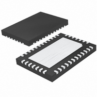
LT3513EUHF#TRPBF Linear Technology, LT3513EUHF#TRPBF Datasheet - Page 18

LT3513EUHF#TRPBF
Manufacturer Part Number
LT3513EUHF#TRPBF
Description
IC REG 5-OUT FOR TFT-LCD 38QFN
Manufacturer
Linear Technology
Datasheet
1.LT3513EUHFPBF.pdf
(22 pages)
Specifications of LT3513EUHF#TRPBF
Applications
Converter, TFT, LCD
Voltage - Input
4.5 ~ 30 V
Number Of Outputs
5
Voltage - Output
0.8 ~ 40 V
Operating Temperature
-40°C ~ 125°C
Mounting Type
Surface Mount
Package / Case
38-QFN
Lead Free Status / RoHS Status
Lead free / RoHS Compliant
Available stocks
Company
Part Number
Manufacturer
Quantity
Price
operaTion
LT3513
below the rated voltage of the capacitor. Be sure to place
the 1µF ceramic as close as possible to the V
pins on the IC for optimal noise immunity.
A final caution is in order regarding the use of ceramic
capacitors at the input. A ceramic input capacitor can
combine with stray inductance to form a resonant tank
circuit. If power is applied quickly (for example by plugging
the circuit into a live power source), this tank can ring,
doubling the input voltage and damaging the LT3513. The
solution is to either clamp the input voltage or dampen the
tank circuit by adding a lossy capacitor (an electrolytic)
in parallel with the ceramic capacitor. For details, see Ap-
plication Note 88.
Soft-Start and Shutdown
The RUN-SS1(Run/Soft-Start) pin is used to place the
switching regulators and the internal bias circuits in shut-
down mode. It also provides a soft-start function, along
with RUN-SS2 and RUN-SS3/4. If the RUN-SS1 pin is
pulled to ground, the LT3513 enters its shutdown mode
with all regulators off and quiescent current reduced to
~30µA. An internal 2µA current source pulls up on the
RUN-SS1, RUN-SS2, and RUN-SS3/4 pins. If the RUN-
SS1 pin reaches ~0.6V, the internal bias circuits start and
the quiescent currents increase to their nominal levels.
If a capacitor is tied from the RUN-SS1, RUN-SS2 or
RUN-SS3/4 pins to ground, then the internal pull-up
current will generate a voltage ramp on these pins. This
voltage clamps the V
and therefore input current during start-up. The RUN-SS1
pin clamps V
RUN-SS3/4 pin clamps the V
for the soft-start capacitors is C
is the value of the largest output capacitor.
V
The V
When the C
18
ON
Pin Considerations
ON
pin is the delayed output for switching regulator 3.
T
pin reaches 1.1V, the output disconnect PNP
C1
, the RUN-SS2 pin clamps V
C
pin, limiting the peak switch current
C3
and V
OUT
/10,000, where C
C4
pins. A good value
IN
C1
and GND
and the
OUT
turns on, connecting V
limited and will protect the LT3513 and input source from
a shorted output.
The V
pin. When V
C
than 1.5V, the V
collector device turns on. If the V
to V
a high V
scanning frequency to improve LCD image quality.
Low Voltage Dropout Linear Regulator
The LT3513 features an output to drive an external NPN
transistor LDO to provide a lower voltage logic supply volt-
age. The output is capable of providing 10mA of current to
the base of the NPN. The output of the LDO is controlled
by the FB5 pin. Choose the resistor values according to:
R8 should be 10k or less to avoid bias current errors.
The internal compensation of the LDO relies on a low ESR
ceramic capacitor between the values of 2.2µF and 20µF .
X7R dielectrics are preferred, followed by X5R, as these
materials retain their capacitance over wide voltage and
temperature ranges.
Printed Circuit Board Layout
For proper operation and minimum EMI, care must be
taken during printed circuit board (PCB) layout. Figure 3
shows the high current paths in the step-down regula-
tor circuit. Note that in the step-down regulators, large,
switched currents flow in the power switch, the catch
diode and the input capacitor. In the step-up regulators,
large, switched currents flow through the power switch,
the switching diode and the output capacitor. In SEPIC and
T
pin is greater than 1.1V. When V
R8 = R7
ON
ON
through a resistor, the V
ON_CLK
pin output is also controlled from the V
ON_CLK
0.625V
V
ON
. V
LDO
ON_CLK
output is disabled and the V
is low, the V
– 1
ON
may be synced to the horizontal
to E3. The V
ON
ON
ONSINK
output will turn on if the
voltage will decay with
ON_CLK
ON
pin is connected
is high, greater
pin is current
ONSINK
ON_CLK
open
3513fc


