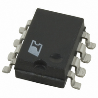
DPA424GN Power Integrations, DPA424GN Datasheet - Page 3

DPA424GN
Manufacturer Part Number
DPA424GN
Description
IC CONV DC-DC DPA SWITCH 8SMD
Manufacturer
Power Integrations
Series
DPA-Switch®r
Specifications of DPA424GN
Applications
Converter, Power Over Ethernet and Telecom Applications
Voltage - Input
16 ~ 75 V
Number Of Outputs
1
Voltage - Output
220V
Operating Temperature
-40°C ~ 125°C
Mounting Type
Surface Mount
Package / Case
8-SMD Gull Wing
Mounting Style
SMD/SMT
For Use With
596-1195 - KIT REF DES DPA 6.6W DC-DC CONV596-1009 - KIT DESIGN ACCELERATOR DC-DC596-1007 - KIT DESIGN ACCELERATOR POE CONV
Lead Free Status / RoHS Status
Lead free / RoHS Compliant
Available stocks
Company
Part Number
Manufacturer
Quantity
Price
Company:
Part Number:
DPA424GN
Manufacturer:
POWER
Quantity:
15 000
Part Number:
DPA424GN
Manufacturer:
POWER
Quantity:
20 000
Part Number:
DPA424GN-TL
Manufacturer:
POWER
Quantity:
20 000
Figure 2.
Pin Functional Description
DRAIN (D) Pin:
High voltage power MOSFET drain output. The internal startup
bias current is drawn from this pin through a switched high-
voltage current source. Internal current limit sense point for
drain current.
CONTROL (C) Pin:
Error amplifi er and feedback current input pin for duty cycle
control. Internal shunt regulator connection to provide internal
bias current during normal operation. It is also used as the
connection point for the supply bypass and auto-restart/
compensation capacitor.
LINE-SENSE (L) Pin:
Input pin for overvoltage (OV), under-voltage (UV) lock out, line
feed-forward with the maximum duty cycle (DC
remote ON/OFF and synchronization. A connection to
SOURCE pin disables all functions on this pin.
EXTERNAL CURRENT LIMIT (X) Pin:
Input pin for external current limit adjustment and remote
ON/OFF. A connection to SOURCE pin disables all functions
on this pin.
FREQUENCY (F) Pin:
Input pin for selecting switching frequency: 400 kHz if
connected to SOURCE pin and 300 kHz if connected to
CONTROL pin.
www.powerint.com
CURRENT LIMIT (X)
FREQUENCY (F)
LINE-SENSE (L)
EXTERNAL
CONTROL (C)
Functional Block Diagram.
R E
Z C
I FB
SHUNT REGULATOR/
ERROR AMPLIFIER
CURRENT
ADJUST
LIMIT
SENSE
LINE
V BG + V T
V BG
+
-
V C
1 V
V I (LIMIT)
ON/OFF
5.8 V
OV/UV
DC MAX
START
SOFT
STOP LOGIC
OSCILLATOR
5.8 V
4.8 V
COMPARATOR
INTERNAL UV
DC MAX
300/400 kHz
MAX
STOP SOFT-
+
-
) reduction,
START
CLOCK
D MAX
SAW
SKIPPING
CYCLE
SOFT START
COMPARATOR
SOURCE (S) Pin:
Output MOSFET source connection for the power return.
Primary side control circuit common and reference point.
Figure 2.
AUTO-RESTART
SHUTDOWN/
HYSTERETIC
PWM
SHUTDOWN
THERMAL
+
-
÷ 8
0
Pin Confi guration (Top View).
1
(TO-263-7C)
R Package
C L X S F
1 2 3 4 5
INTERNAL
SUPPLY
S
R
D
7
Q
(See layout considerations)
C
X
L
F
G Package (SMD-8)
Tab internally connected
P Package (DIP-8)
2
3
4
1
DPA422-426
CONTROLLED
GATE DRIVER
to SOURCE pin
CURRENT LIMIT
COMPARATOR
TURN-ON
BLANKING
+
-
LEADING
EDGE
PI-2760-070501
8
5
7
6
PI-4030-110507
S
S
D
S
DRAIN (D)
SOURCE (S)
Rev. S 12/07
3


