L6714 STMicroelectronics, L6714 Datasheet - Page 59

L6714
Manufacturer Part Number
L6714
Description
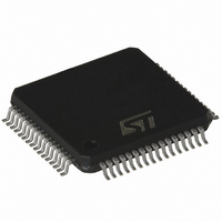
IC CTRLR 4PH W/DRIVERS 64-TQFP
Manufacturer
STMicroelectronics
Datasheet
1.L6714TR.pdf
(70 pages)
Specifications of L6714
Applications
Controller, Intel VR10, VR11, AMD CPU
Voltage - Input
12V
Number Of Outputs
4
Voltage - Output
0.3 ~ 1.6 V
Operating Temperature
0°C ~ 70°C
Mounting Type
Surface Mount
Package / Case
64-TQFP Exposed Pad, 64-eTQFP, 64-HTQFP, 64-VQFP
Mounting Style
SMD/SMT
Case
QFP
Lead Free Status / RoHS Status
Lead free / RoHS Compliant
Available stocks
Company
Part Number
Manufacturer
Quantity
Price
Company:
Part Number:
L6714TR
Manufacturer:
WYC
Quantity:
22 140
Part Number:
L6714TR
Manufacturer:
ST
Quantity:
20 000
L6714
21.1
Compensation network can be simply designed placing
frequency
1/10th of the switching frequency F
Compensation network guidelines
The Compensation Network design assures to having system response according to the
cross-over frequency selected and to the output filter considered: it is anyway possible to
further fine-tune the compensation network modifying the bandwidth in order to get the best
response of the system as follow
●
●
●
Having the fastest compensation network gives not the confidence to satisfy the
requirements of the load: the inductor still limits the maximum dI/dt that the system can
afford. In fact, when a load transient is applied, the best that the controller can do is to
“saturate” the duty cycle to its maximum (d
dV/dt is then limited by the inductor charge / discharge time and by the output capacitance.
In particular, the most limiting transition corresponds to the load removal since the inductor
results being discharged only by V
appliance).
Referring to
improvements unless the output filter changes: only modifying the main inductors ot the
output capacitance improves the system response.
Figure 24. R
Increase R
Decrease R
Increase C
phase margin.
T
Figure
as desired obtaining (always considering that
F
-C
F
F
F
F
to increase the system bandwidth accordingly;
to move
R
to decrease the system bandwidth accordingly;
impact on bandwidth.
24-left, further tuning the Compensation network cannot give any
F
[dB]
R
K
F
=
dB
R
------------------------------------ -
F
FB
to low frequencies increasing as a consequence the system
V
IN
(See Figure
LC
V
OUT
C
SW
OSC
=
F
G
):
C
(while it is charged by d
F
LOOP
F
ESR
5
-- -
4
=
MAX
(s)
----------------------- -
C
24):
) or minimum (0) value. The output voltage
T
R
O
F
---------------------------------------------------------- -
N
--- -
N
L
System control loop compensation
R
DROOP
F
R
=
F
L
LC
T
might be not higher than
MAX
and imposing the cross-over
+
Z
ESR
F
V
(s)
T
IN
-V
OUT
during a load
59/70


