PM6641 STMicroelectronics, PM6641 Datasheet - Page 23

PM6641
Manufacturer Part Number
PM6641
Description
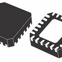
IC MONO VR DDR2/3 PC VFQFPN-48
Manufacturer
STMicroelectronics
Datasheet
1.PM6641TR.pdf
(47 pages)
Specifications of PM6641
Applications
Converter, DDR2, DDR3
Voltage - Input
2.7 ~ 5.5 V
Number Of Outputs
3
Voltage - Output
0.8 ~ 5.5 V
Operating Temperature
0°C ~ 85°C
Mounting Type
Surface Mount
Package / Case
48-VFQFN
Output Voltage
0.9 V
Output Current
3 A
Input Voltage
2.7 V to 5.5 V
Switching Frequency
1000 KHz
Operating Temperature Range
- 40 C to + 125 C
Mounting Style
SMD/SMT
For Use With
497-8425 - KIT EVAL PM6641 CHIPSET/DDR2/3
Lead Free Status / RoHS Status
Lead free / RoHS Compliant
Available stocks
Company
Part Number
Manufacturer
Quantity
Price
Company:
Part Number:
PM6641
Manufacturer:
BITECHNOL
Quantity:
2 000
Part Number:
PM6641
Manufacturer:
ST
Quantity:
20 000
Company:
Part Number:
PM6641TR
Manufacturer:
STM
Quantity:
35 839
PM6641
current mode loop to avoid sub-harmonic instability with duty cycle greater than 50%, is
internally implemented and no further external components are required.
The chipset supply is able to source the following average and peak currents, assuming
1 A peak-to-peak inductor current ripple:
Table 9.
The peak current and the inductor ripple must be carefully evaluated in order to choose the
right current limit protection; this feature is performed by sensing the internal high side
MOSFET current and can be decreased by inserting an external resistor between CSNS pin
and AGND (see
Both rails are able to protect the load from over-voltage and under-voltage protection, which
avoid the output to be higher than 120% or lower than 60% of the nominal value (see
Chapter 7.11.1: Output overvoltage on page 33
on page 33
When the EN_1S5 or EN_1S05 pin goes high the respective rail is turned on and the output
voltage soft-start is performed by slowly charging the rail output capacitor; this behavior is
achieved because the loop voltage reference is increased linearly from zero up to 0.8V (see
Chapter 7.6: Outputs soft-start on page 28
EN_1S05 pin goes low, the respective rail output capacitor is discharged through internal
discharge MOSFET and, at the end of the capacitor discharge, the low side power MOSFET
is finally closed (see
Each rail has a dedicated pin to assert if its output voltage is not in the power good window,
i.e. if the output voltage drops 10% below or rises 10% above the nominal regulated value.
These power good signals (PG_1S5 and PG_1S05 pins) are open drain outputs, tied to
GND in the following conditions:
●
●
●
The PG_1S5 and PG_1S05 pins can sink current up to 4 mA when it’s asserted low.
Chipset supply rail [V]
When the rail output voltage is outside +/- 10% range from nominal value
When a protection (UV, OV, thermal) has been triggered
When the regulator is in soft-start.
section for details).
Chipset supply currents
1.05
1.5
Chapter 7.10: Peak current limit on page 31
Chapter 7.7: Outputs soft-end on page 29
Doc ID 13510 Rev 3
Average current [A]
section for details). When the EN_1S5 or
1.5
2.1
and
Chapter 7.11.2: Output under voltage
for details).
section for details).
Peak current [A]
Device description
3.0
4.0
23/47


