PM6641 STMicroelectronics, PM6641 Datasheet - Page 29

PM6641
Manufacturer Part Number
PM6641
Description
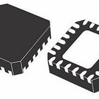
IC MONO VR DDR2/3 PC VFQFPN-48
Manufacturer
STMicroelectronics
Datasheet
1.PM6641TR.pdf
(47 pages)
Specifications of PM6641
Applications
Converter, DDR2, DDR3
Voltage - Input
2.7 ~ 5.5 V
Number Of Outputs
3
Voltage - Output
0.8 ~ 5.5 V
Operating Temperature
0°C ~ 85°C
Mounting Type
Surface Mount
Package / Case
48-VFQFN
Output Voltage
0.9 V
Output Current
3 A
Input Voltage
2.7 V to 5.5 V
Switching Frequency
1000 KHz
Operating Temperature Range
- 40 C to + 125 C
Mounting Style
SMD/SMT
For Use With
497-8425 - KIT EVAL PM6641 CHIPSET/DDR2/3
Lead Free Status / RoHS Status
Lead free / RoHS Compliant
Available stocks
Company
Part Number
Manufacturer
Quantity
Price
Company:
Part Number:
PM6641
Manufacturer:
BITECHNOL
Quantity:
2 000
Part Number:
PM6641
Manufacturer:
ST
Quantity:
20 000
Company:
Part Number:
PM6641TR
Manufacturer:
STM
Quantity:
35 839
PM6641
7.7
7.8
Outputs soft-end
When the switching regulator enable pin (EN_1S8 for the VDDQ section, EN_1S5 and
EN_1S05 for chipset sections) goes down or when UV or thermal protections are detected,
the switching regulator output capacitor is actively discharged through a dedicated
discharge MOSFET of about 25 Ω typical resistance.
The PM6641 DDR supply allows choosing between two different output discharge
behaviors, involving the VDDQ (1S8) switching rail, VTT LDO termination and VTTREF
reference buffered voltage: the tracking discharge and the non-tracking discharge. This
selection is set by tying the discharge pin (DSCG) to AVCC (tracking discharge enabled) or
to AGND (tracking discharge disabled).
When the 1.8 V rail is turned off (EN_1S8 goes low) and non-tracking discharge is active
(DSCG is low), or when UV or thermal protections are detected, the VDDQ and VTT rails
and the VTTREF buffer are discharged by internal discharge MOSFETs, through the
VSW_1S8, VTTFB and VTTREF pins respectively. VTT termination output capacitor is
discharged through 25 Ω dedicated MOSFET whereas VTTREF output capacitor is
discharged through 200 Ω dedicated MOSFET.
When the 1.8 V rail is turned off (EN_1S8 goes low) and tracking discharge is selected
(DSCG is high), tracking discharge takes place:
●
●
When the VTT LDO and VTTREF reach a voltage threshold of about 200-300 mV, the
device switches to non-tracking discharge mode and the internal discharge MOSFETs are
turned on.
Switching frequency selection
SET_SWF (pin 2) allows to vary the internal oscillator switching frequency, in the range of
500 kHz
70 k Ω
The following table summarizes the output resistor – switching frequency correspondence:
Table 10.
When SET_SWF is tied to AVCC the internal reference is chosen and each regulator
performs a typical 750 kHz switching frequency.
The 1.8 V rail regulator is discharged by internal MOSFET
The 0.9 V VTT LDO and VTTREF work in tracking with the half of 1.8 V rail
140k Ω .
R
SET_SWF
1 MHz, by connecting this pin to AGND through a resistor between
Typical values for switching frequency selection
140
100
70
(kΩ)
Doc ID 13510 Rev 3
Approx. switching frequency (kHz)
1000
500
670
Device description
29/47


