ISL6422EVEZ Intersil, ISL6422EVEZ Datasheet

IC VREG DUAL LNB W/I2C 38EPTSSOP

ISL6422EVEZ

Manufacturer Part Number
ISL6422EVEZ
Description
IC VREG DUAL LNB W/I2C 38EPTSSOP
Manufacturer
Intersil
Datasheet

Specifications of ISL6422EVEZ

Applications
Converter, Satellite Set-Top Box Designs
Voltage - Input
8 ~ 14 V
Number Of Outputs
2
Voltage - Output
13.3 ~ 18.3 V, 14.3 ~ 19.3 V
Operating Temperature
-20°C ~ 85°C
Mounting Type
Surface Mount
Package / Case
38-TSSOP Exposed Pad, 38-eTSSOP, 38-HTSSOP
Lead Free Status / RoHS Status
Lead free / RoHS Compliant

Available stocks

Company
Part Number
Manufacturer
Quantity
Price
Part Number:
ISL6422EVEZ
Manufacturer:
INTERSIL
Quantity:
6 221
Part Number:
ISL6422EVEZ
Manufacturer:
HAR
Quantity:
20 000
Dual Output LNB Supply and Control
Voltage Regulator with I
Advanced Satellite Set-Top Box Designs
The ISL6422 is a highly integrated voltage regulator and
interface IC, specifically designed for supplying power and
control signals from advanced satellite set-top box (STB)
modules to the low noise blocks (LNBs) of two antenna
ports. The device is consists of two independent
current-mode boost PWMs and two low-noise linear
regulators along with the circuitry required for 22kHz tone
generation, modulation and I
makes the total LNB supply design simple, efficient and
compact with low external component count.
Two independent current-mode boost converters provide the
linear regulators with input voltages that are set to the final
output voltages, plus typically 0.8V to insure minimum power
dissipation across each linear regulator. This maintains
constant voltage drops across each linear pass element
while permitting adequate voltage range for tone injection.
The final regulated output voltages are available at two
output terminals to support simultaneous operation of two
antenna ports for dual tuners. The outputs for each PWM
can be controlled in two ways:
• Full control from I
• Set the I
All the functions on this IC are controlled via the I
writing 8-bit words onto the System Registers (SR). The
same register can be read back, and 4-bits per output will
report the diagnostic status. Separate enable commands sent
on the I
each PWM and linear combination, disabling the output into
shutdown mode. Each output channel is capable of providing
750mA of continuous current. The overcurrent limit can be
digitally programmed.
The External modulation input EXTM1, EXTM2 can accept a
modulated Diseqc command and transfer it symmetrically to
the output. Alternatively, the EXTM1 or EXTM2 pin can be
used to modulate the continuous internal tone.
The FLT pin serves as an interrupt for the processor when
an over temperature, overcurrent or backwards overcurrent
fault conditions is detected by the LNB controller or when
both channels are disabled by the I
nature of the fault can be read of the I
and VBOT12 bits, or
higher range (18V/19V) with the SELVTOP1 or
SELVTOP2 pin.
2
C bus provide independent standby mode control for
2
C to the lower range (13V/14V) and switch to the
2
C using the VTOP1, VTOP2, VBOT1,
®
2
C device interface. The device
1
2
2
C Interface for
Data Sheet
C EN bits set low. The
2
C registers.
2
C bus by
1-888-INTERSIL or 1-888-468-3774
CAUTION: These devices are sensitive to electrostatic discharge; follow proper IC Handling Procedures.
Features
• Single Chip Power Solution
• Switch-Mode Power Converter for Lowest Dissipation
• Output Back Bias Capability of 28V
• I
• Four level Slave Address 0001 00XX
• 2.5V, 3.3V, 5V Logic Compatible
• External Pins to Toggle Between V and H Polarization.
• Supports DiSEqC 2.0 Protocol
• Built-In Tone Oscillator Factory Trimmed to 22kHz
• Internal Over-Temperature Protection and Diagnostics
• Internal OV, UV, Overload and Over-Temperature Flags
• FLT Signal
• LNB Short-Circuit Protection and Diagnostics
• QFN, EPTSSOP Packages
• Pb-Free Plus Anneal Available (RoHS Compliant)
Applications
• LNB Power Supply and Control for Satellite Set-Top Box
Ordering Information
*Add “-T” suffix for tape and reel.
NOTE: Intersil Pb-free plus anneal products employ special Pb-free
material sets; molding compounds/die attach materials and 100% matte tin
plate termination finish, which are RoHS compliant and compatible with
both SnPb and Pb-free soldering operations. Intersil Pb-free products are
MSL classified at Pb-free peak reflow temperatures that meet or exceed
the Pb-free requirements of IPC/JEDEC J STD-020.
PART NUMBER
ISL6422ERZ*
ISL6422EVEZ* ISL6422 EVEZ -20 to+ 85 38 Ld EPTSSOP M38.173B
- True Dual Operation for 2-Tuner/2-Dish Applications
- Both Outputs May be Enabled Simultaneously at
- Integrated DC/DC Converter and I
- Boost PWMs with >92% Efficiency
- Selectable 13.3V or 18.3V Outputs
- Digital Cable Length Compensation (1V)
- I
- Facilitates DiSEqC (EUTELSAT) Encoding
- External Modulation Input
(Visible on I
2
C Compatible Interface for Remote Device Control
Maximum Power
(Note)
2
August 10, 2007
C and Pin controllable output
All other trademarks mentioned are the property of their respective owners.
|
Intersil (and design) is a registered trademark of Intersil Americas Inc.
2
C)
Copyright Intersil Americas Inc. 2006, 2007. All Rights Reserved
ISL6422 ERZ
MARKING
PART
-20 to +85 40 Ld 6x6 QFN
RANGE
TEMP.
(°C)
2
C Interface
PACKAGE
ISL6422
(Pb-free)
FN9190.2
L40.6x6
DWG. #
PKG.

Related parts for ISL6422EVEZ

ISL6422EVEZ Summary of contents

Page 1

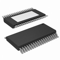
... Ordering Information PART NUMBER (Note) ISL6422ERZ* ISL6422EVEZ* ISL6422 EVEZ -20 to EPTSSOP M38.173B *Add “-T” suffix for tape and reel. NOTE: Intersil Pb-free plus anneal products employ special Pb-free material sets; molding compounds/die attach materials and 100% matte tin plate termination finish, which are RoHS compliant and compatible with both SnPb and Pb-free soldering operations ...

Page 2

... SELVTOP2 VSW2 3 36 TCAP2 35 NC GATE2 4 PGND2 5 34 VOUT2 EXTM2 6 33 TDIN2 SGND 7 32 TDOUT2 31 CPVOUT FLT 8 SDA 9 30 CPSWOUT ISL6422EVEZ SCL 10 29 CPSWIN ADDR0 11 28 VCC 27 TDOUT1 ADDR1 12 EXTM1 13 26 TDIN1 BYP 14 25 VOUT1 24 AGND PGND1 15 GATE1 16 23 TCAP1 VSW1 ...

Page 3

Block Diagram OLF1 OVERCURRENT COUNTER PROTECTION DCL1 LOGIC SCHEME 1 PWM OC1 LOGIC GATE1 12 Q CLK1 S PGND1 11 ILIM1 CS - AMP CS1 ∑ 15 SLOPE COMPENSATION TDOUT1 23 - TONE TXT1 DECODER VREF1 TDIN1 22 VSW1 14 ...

Page 4

Typical Application Schematic QFN ...

Page 5

... EPTSSOP Package . . . . . . . . . . . . . . . QFN Package Maximum Junction Temperature (Note +150°C Maximum Storage Temperature Range . . . . . . . . . . -40°C to +150°C Pb-free reflow profile . . . . . . . . . . . . . . . . . . . . . . . . . .see link below http://www.intersil.com/pbfree/Pb-FreeReflow.aspOperating Temperature Range . . . . . . . . . . . . . . . . . . . . . . . . . . -20°C to +85°C = -20°C to +85°C, unless otherwise noted. Typical values are SYMBOL TEST CONDITIONS ...

Page 6

Electrical Specifications V = 12V VTOP1 = VTOP2 = L, ENT1 = ENT2 = L, DCL = L, DSQIN1 = DSQIN2 = L, I noted. See “ISL6422 Software Description” on page 12 for I PARAMETER Dynamic Output Current ...

Page 7

Electrical Specifications V = 12V VTOP1 = VTOP2 = L, ENT1 = ENT2 = L, DCL = L, DSQIN1 = DSQIN2 = L, I noted. See “ISL6422 Software Description” on page 12 for I PARAMETER TXT1 AND TXT2, ...

Page 8

Tone Waveform ENT1 MSEL1 EXTM1/2 PIN VOUT1/2 PIN 22kHz 22kHz Internal Tone t = 10µs typ r NOTES: 9. The logic presented to the signal pins TXT1 and TXT2 changes the decoder threshold during ...

Page 9

Functional Pin Descriptions SYMBOL SDA Bidirectional data from/ SCL Clock from I C bus. VSW1 and VSW2 Input of the linear post-regulator. PGND1 and PGND2 Dedicated ground for the output gate driver of respective PWM. CS1 and CS2 ...

Page 10

Functional Description The ISL6422 dual output voltage regulator makes an ideal choice for advanced satellite set-top box and personal video recorder applications. Both supply and control voltage outputs for two low-noise blocks (LNBs) are available simultaneously in any output configuration. ...

Page 11

Current Limiting The dynamic back current limit block has five thresholds that can be selected by the following bits of the SR. • ISEL1H and ISEL2H • ISEL1L and ISEL2L • ISEL1R and ISEL2R See Table 8 and Table 9 ...

Page 12

Data Validity The data on the SDA line must be stable during the HIGH period of the clock. The HIGH or LOW state of the data line can change only when the clock signal on the SCL line is LOW. ...

Page 13

TABLE 6. CONTROL REGISTER 4 (SR4 SR4H SR4M SR4L EN1 X TABLE 7. STATUS REGISTER 5 (SR5 SR5H SR5M SR5L X CABF2 ...

Page 14

SR3H SR3M SR3L DCL1 VSPEN1 ISEL1R ISEL1H ISEL1L ...

Page 15

SR5H SR5M SR5L CABF2 OUVF2 ...

Page 16

SR8H SR8M SR8L EN2 ...

Page 17

ADDR0 and ADDR1 Pins Connecting either ADDR0 or ADDR1 to GND, the chip I interface address is 0001000, but it is possible to choose between four different addresses simply by setting the logic as indicated in Table 19 ...

Page 18

Package Outline Drawing L40.6x6 40 LEAD QUAD FLAT NO-LEAD PLASTIC PACKAGE Rev 3, 10/06 6.00 6 PIN 1 INDEX AREA (4X) 0.15 TOP VIEW ( TYP ) ( TYPICAL RECOMMENDED LAND PATTERN 18 ...

Page 19

... Accordingly, the reader is cautioned to verify that data sheets are current before placing orders. Information furnished by Intersil is believed to be accurate and reliable. However, no responsibility is assumed by Intersil or its subsidiaries for its use; nor for any infringements of patents or other rights of third parties which may result from its use ...

Related keywords