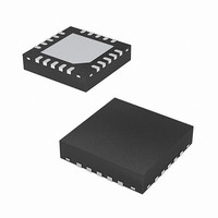
EL7586ILZ Intersil, EL7586ILZ Datasheet - Page 16

EL7586ILZ
Manufacturer Part Number
EL7586ILZ
Description
IC POWER SUPPLY TFT-LCD 20-QFN
Manufacturer
Intersil
Datasheet
1.EL7586AILZ-T13.pdf
(21 pages)
Specifications of EL7586ILZ
Applications
Converter, TFT, LCD
Voltage - Input
3 ~ 5 V
Number Of Outputs
4
Voltage - Output
5.5 ~ 20 V
Operating Temperature
-40°C ~ 85°C
Mounting Type
Surface Mount
Package / Case
20-VQFN Exposed Pad, 20-HVQFN, 20-SQFN, 20-DHVQFN
Lead Free Status / RoHS Status
Lead free / RoHS Compliant
Available stocks
Company
Part Number
Manufacturer
Quantity
Price
Part Number:
EL7586ILZ
Manufacturer:
INTERSIL
Quantity:
20 000
The following equation gives the boundary between
discontinuous and continuous boost operation. For
continuous operation (LX switching every clock cycle) we
require that:
I(A
where the duty cycle, D = (A
For example, with V
12V we find continuous operation of the boost converter can
be guaranteed for:
L = 10µH and I(A
L = 6.8µH and I(A
L = 3.3µH and I(A
Charge Pump Output Capacitors
Ceramic capacitors with low ESR are recommended. With
ceramic capacitors, the output ripple voltage is dominated by
the capacitance value. The capacitance value can be
chosen by the following equation:
C
where f
Start-Up Sequence
Figure 33 and 34 show a detailed start-up sequence
waveform. For a successful power up, there should be six
peaks at V
latch off until either EN is toggled or the input supply is
recycled.
When the input voltage is higher than 2.5V, an internal
current source starts to charge C
using a fast ramp followed by a slow ramp. During the initial
slow ramp, the device checks whether there is a fault
condition. If no fault is found, C
first peak and V
During the second ramp, the device checks the status of
V
ramp, PG output goes low and enables the input protection
PMOS Q1. Q1 is a controlled FET used to prevent in-rush
current into V
Its rate of turn on is controlled by C
detected, M1 will turn off and disconnect the inductor from
V
With the input protection FET on, NODE1 (See Typical
Application Diagram) will rise to ~V
not enabled so V
output diode. Hence, there is a step at V
part of the start-up sequence. If this step is not desirable, an
external PMOS FET can be used to delay the output until the
boost is enabled internally. The delayed output appears at
A
VDD
OUT
REF
IN
VDD
.
.
≥
and over temperature. At the peak of the second
_load) > D*(1-D)*V
OSC
------------------------------------------------------
2
×
CDLY
V
RIPPLE
is the switching frequency.
BOOST
I
OUT
. When a fault is detected, the device will
REF
BOOST
VDD
VDD
VDD
×
IN
turns on.
before V
) > 61mA
f
) > 89mA
) > 184mA
OSC
= 5V, F
rises to V
IN
/(2*L*F
VDD
16
OSC
BOOST
CDLY
CDLY
- V
IN
= 1.0MHz and A
OSC
o
IN
IN
. When a fault is
-V
is discharged after the
. Initially the boost is
is enabled internally.
)/A
DIODE
to an upper threshold
)
BOOST
VDD
through the
during this
VDD
EL7586, EL7586A
=
For the EL7586, V
beginning of the third ramp. The soft-start ramp depends on
the value of the C
soft-start time is ~2ms.
The EL7586A is the same as the EL7586 except V
V
When a fault is detected, the outputs and the input protection
will turn off but V
V
peak, the open drain o/p DELB goes low to turn on the
external PMOS Q4 to generate a delayed V
V
PG, V
Fault Protection
Once the start-up sequence is complete, the voltage on the
C
detected or the EN pin is disabled. If a fault is detected, the
voltage on C
disabled until the power is recycled or enable is toggled.
Component Selection for Start-Up Sequencing and
Fault Protection
The C
to stabilize the V
22nF to 1µF and should not be more than five times the
capacitor on C
The C
range from 47nF minimum to several microfarads - only
limited by the leakage in the capacitor reaching µA levels.
C
above). Note with 220nF on C
typically 50ms and the use of a larger/smaller value will vary
this time proportionally (e.g. 1µF will give a fault time-out
period of typically 230ms).
Fault Sequencing
The EL7586 and EL7586A have advanced fault detection
systems which protects the IC from both adjacent pin shorts
during operation and shorts on the output supplies.
A high quality layout/design of the PCB, in respect of
grounding quality and decoupling is necessary to avoid
falsely triggering the fault detection scheme - especially
during start-up. The user is directed to the layout guidelines
and component selection sections to avoid problems during
initial evaluation and prototype PCB generation.
LOGIC
OFF
ON
DLY
DEL
is enabled at the beginning of the sixth ramp. A
OFF
capacitor remains at 1.15V until either a fault is
REF
DEL
turns on at the start of the fourth peak. At the fifth
should be at least 1/5 of the value of C
turn on when input voltage (V
, DELB and V
capacitor is typically 220nF and has a usable
capacitor is typically set at 220nF and is required
DLY
DEL
REF
REF
rises to 2.4V at which point the chip is
DLY
BOOST
to ensure correct start-up operation.
output. The range of C
will stay on.
capacitor. For C
ON
and V
are checked at end of this ramp.
DEL
LOGIC
the fault time-out will be
DD
DLY
soft-start at the
) exceeds 2.5V.
of 220nF, the
BOOST
REF
REF
January 17, 2006
is from
(See
REF
output.
VDD
FN9210.2
and
,


