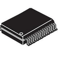
MCZ34702EWR2 Freescale Semiconductor, MCZ34702EWR2 Datasheet - Page 24

MCZ34702EWR2
Manufacturer Part Number
MCZ34702EWR2
Description
IC PWR SUPPLY 3A SW 32-SOIC
Manufacturer
Freescale Semiconductor
Datasheet
1.MC34702EK.pdf
(39 pages)
Specifications of MCZ34702EWR2
Applications
Controller, Power QUICC™ I, II
Voltage - Input
2.8 ~ 6 V
Number Of Outputs
2
Voltage - Output
7.75V, 0.8 ~ 6 V
Operating Temperature
-40°C ~ 85°C
Mounting Type
Surface Mount
Package / Case
32-SOIC (7.5mm Width)
Output Current
3 A
Input Voltage
2.8 V to 6 V
Switching Frequency
300 KHz
Mounting Style
SMD/SMT
Duty Cycle (max)
95 %
Lead Free Status / RoHS Status
Lead free / RoHS Compliant
Standard Power Sequencing Control
LDO (LDO pin) and the switcher (VOUT pin) outputs as
follows:
Inverted Power Sequencing Control
switcher (VOUT pin) and LDO (LDO pin) outputs as follows:
24
34702
FUNCTIONAL DEVICE OPERATION
OPERATIONAL MODES
1. LDO > VOUT + 1.9V, turn off LDO. The LDO can be
2. LDO > VOUT + 2.0V, shunt LDO to ground. If turning
3. LDO < VOUT + 1.9V cancel (2).
4. LDO < VOUT + 1.8V, cancel (1) above, re-enable LDO.
5. LDO < VOUT - 0.1V, turn off switcher. The switcher
6. LDO < VOUT - 0.3V, turn on Sync (LS) MOSFET and
7. LDO > VOUT - 0.3V, cancel (6).
8. LDO > VOUT - 0.1V, cancel (5). Normal operation
1. VOUT > LDO + 1.8V, turn off VOUT . The switcher
2. VOUT > LDO + 2.0V, shunt VOUT to ground. If turning
3. VOUT < LDO + 1.8V, cancel (1) and (2) above, re-
Comparators monitor voltage differences between the
Comparators monitor voltage differences between the
forced off. This occurs whenever the LDO output
voltage exceeds the switcher output voltage by more
than 1.9V.
off the LDO is insufficient and the LDO output voltage
exceeds the switcher output voltage by more than
2.0V, a 1.5Ω shunt MOSFET is turned on that
discharges the LDO load capacitor to ground. The
shunt MOSFET is used for switcher output shorts to
ground and for power down in case of VIN1 ≠ VIN2
with the switcher output falling faster than the LDO.
Normal operation resumes when the LDO output
voltage is less than 1.8V above the switcher output
voltage.
can be forced off. This occurs whenever the LDO is
less than VOUT - 0.1V.
1.5
MOSFET is forced off and the Sync MOSFET is forced
on. This occurs when the switcher output voltage
exceeds the LDO output by more than 300mV.
resumes when LDO < VOUT - 0.1V .
VOUT can be forced off. This occurs whenever the
VOUT output voltage exceeds the LDO output voltage
by more than 1.8V.
off the switcher VOUT is insufficient and the VOUT
output voltage exceeds the LDO output voltage by
more than 2.0V, a 1.5Ω shunt MOSFET and the
switcher synchronous MOSFET are turned on to
discharge the VOUT load capacitor to ground. The
shunt MOSFET and synchronous MOSFET are used
for LDO output shorts to ground and for power-down in
case of VIN1 ≠ VIN2 with LDO output falling faster than
the VOUT .
enable VOUT . Normal operation resumes when the
Ω
VOUT sink MOSFET. The buck high side
STANDARD OPERATING MODE
Single 3.3V Supply, VIN = VIN1 = VIN2 = 3.3V
switcher supplies core voltage (e.g., 1.5V nominal), and the
LDO operates independently (see
Power sequencing depends only on the normal switcher
intrinsic operation to control the buck high side MOSFET.
Power-up
point and the buck high side MOSFET is on. In order not to
exceed the 2.1V differential requirement between the I/O
(VIN) and the core (VOUT), the switcher must start up at 2.1V
or less and be able to maintain the 2.1V or less differential.
The maximum slew rate for V
Power-down
therefore, the buck high side MOSFET is on. In the case
where VOUT is falling faster than VIN, the buck high side
MOSFET attempts to maintain VOUT. In the case where VIN
is falling faster than VOUT, the buck high side MOSFET is
also on, and the VOUT load capacitor is discharged through
the buck high side MOSFET to VIN. Thus, provided VIN does
not fall too fast, the core voltage (VOUT) does not exceed the
I/O voltage (VIN) by more than a maximum of 0.4V.
Shorted Load
4. VOUT < LDO + 2.0V, cancel (2)
5. VOUT < LDO - 0.2V, turn off LDO. The LDO can be
6. VOUT < LDO - 0.3V, turn on the 1.5
7. VOUT < LDO - 0.2V, cancel (6).
8. VOUT < LDO - 0.1V, cancel (5). Normal operation
1. VOUT shorted to ground. This causes the I/O voltage
2. VIN shorted to ground. Until the switcher load
3. VOUT shorted to supply. No load protection. 34702 is
The 3.3V supplies the microprocessor I/O voltage, the
When VIN is rising, initially VOUT is below the regulation
When VIN is falling, VOUT falls below the regulation point;
VOUT output voltage is less than 1.8V above the LDO
output voltage.
forced off. This occurs whenever the VOUT is less than
VLDO - 0.2V.
MOSFET. This occurs when the LDO output voltage
exceeds the VOUT output by more than 300mV.
resumes when VOUT > LDO - 0.1V.
to exceed the core voltage by more than 2.1V. No load
protection.
capacitance is discharged, the core voltage exceeds
the I/O voltage by more than 0.4V. By the intrinsic
operation of the switcher, the load capacitor is
discharged rapidly through the buck high side
MOSFET to VIN.
protected by current limit and thermal shutdown.
Analog Integrated Circuit Device Data
IN
is 1.0V/ms.
Figure
Freescale Semiconductor
Ω
17, page 22).
LDO sink


