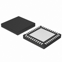
NCP4200MNR2G ON Semiconductor, NCP4200MNR2G Datasheet - Page 12

NCP4200MNR2G
Manufacturer Part Number
NCP4200MNR2G
Description
IC CONV SYNC BUCK PMBUS 40QFN
Manufacturer
ON Semiconductor
Datasheet
1.NCP4200MNR2G.pdf
(32 pages)
Specifications of NCP4200MNR2G
Applications
Converter, Intel VR11, VR11.1
Voltage - Input
1.7 ~ 24 V
Number Of Outputs
1
Voltage - Output
0.375 ~ 1.8 V
Operating Temperature
0°C ~ 85°C
Mounting Type
Surface Mount
Package / Case
40-VFQFN Exposed Pad
Output Voltage
0.375 V to 1.6 V
Output Current
500 uA
Input Voltage
1.7 V to 24 V
Switching Frequency
0.25 MHz to 6 MHz
Operating Temperature Range
0 C to + 85 C
Mounting Style
SMD/SMT
Duty Cycle (max)
100 %
Isolated/non-isolated
Non Isolated
Lead Free Status / RoHS Status
Lead free / RoHS Compliant
Available stocks
Company
Part Number
Manufacturer
Quantity
Price
Company:
Part Number:
NCP4200MNR2G
Manufacturer:
PHILIPS
Quantity:
124
NCP4200.
Phase Detection
phase relationship is determined by the internal circuitry that
monitors the PWM outputs. Normally, the NCP4200
operates as a 4−phase PWM controller.
To operate as a 3−Phase Controller: connect PWM4 to V
To operate as a 2−Phase Controller: connect PWM3 and
PWM4 to V
To operate as a single phase controller: connect PMW2,
PWM3, and PWM4 to V
and PWM2 pins sink approximately 100 mA each. An
internal comparator checks each pin’s voltage vs. a threshold
of 3.0 V. If the pin is tied to V
Otherwise, an internal current sink pulls the pin to GND,
which is below the threshold. PWM1 is low during the phase
detection interval that occurs during the first six clock cycles
of TD2. After this time, if the remaining PWM outputs are
not pulled to V
they function as normal PWM outputs. If they are pulled to
V
are put into a high impedance state.
driving fast response external gate drivers such as the
ADP3121. Because each phase is monitored independently,
operation approaching 100% duty cycle is possible. In
addition, more than one output can be on at the same time to
allow overlapping phases.
Master Clock Frequency
external resistor connected from the RT pin to ground. The
frequency follows the graph in Figure 3. To determine the
frequency per phase, the clock is divided by the number of
CC
Figure 8 shows typical startup waveforms for the
During startup, the number of operational phases and their
Prior to soft−start, while EN is high the PWM4, PWM3
The PWM outputs are logic−level devices intended for
The clock frequency of the NCP4200 is set with an
, the 100 mA current source is removed, and the outputs
Figure 8. Typical Startup Waveforms
CC
.
CC
, the 100 mA current sink is removed, and
CC
.
CC
, it is above the threshold.
http://onsemi.com
CC
.
12
phases in use. If all phases are in use, divide by 4. If 2 phases
are in use then divide by 2.
Output Voltage Differential Sensing
accuracy VID DAC and reference, and a low offset error
amplifier. This maintains a worst−case specification of
±9 mV differential sensing error over its full operating
output voltage and temperature range. The output voltage is
sensed between the FB pin and FBRTN pin. FB is connected
through a resistor, R
remote sense pin of the microprocessor. FBRTN is
connected directly to the remote sense ground point. The
internal VID DAC and precision reference are referenced to
FBRTN, which has a minimal current of 70 mA to allow
accurate remote sensing. The internal error amplifier
compares the output of the DAC to the FB pin to regulate the
output voltage.
Output Current Sensing
Amplifier (CSA) to monitor the total output current for
proper voltage positioning vs. load current, for the I
output and for current limit detection. Sensing the load
current at the output gives the total real time current being
delivered to the load, which is an inherently more accurate
method than peak current detection or sampling the current
across a sense element such as the low−side MOSFET. This
amplifier can be configured in several ways, depending on
the objectives of the system, as follows:
•
•
•
pin, which is connected to the average output voltage. The
inputs to the amplifier are summed together through
resistors from the sensing element, such as the switch node
side of the output inductors, to the inverting input CSSUM.
The feedback resistor between CSCOMP and CSSUM sets
the gain of the amplifier and a filter capacitor is placed in
parallel with this resistor. The gain of the amplifier is
programmable by adjusting the feedback resistor. This
difference signal is used internally to offset the VID DAC
for voltage positioning. This difference signal can be
adjusted between 50% and 150% of the external value using
the I
(0xDF) commands. The difference between CSREF and
CSCOMP is used as a differential input for the current limit
comparator.
is designed to have a low offset input voltage. Also, the
sensing gain is determined by external resistors to make it
extremely accurate.
The NCP4200 combines differential sensing with a high
The NCP4200 provides a dedicated Current Sense
The positive input of the CSA is connected to the CSREF
To provide the best accuracy for sensing current, the CSA
Output inductor DCR sensing without a thermistor for
lower cost.
Output inductor DCR sensing with a thermistor for
improved accuracy with inductor temperature tracking.
Sense resistors for highest accuracy measurements.
2
C Load−line Calibration (0xDE) and Load−line Set
B
, to the regulation point, usually the
MON


