NCP4200MNR2G ON Semiconductor, NCP4200MNR2G Datasheet - Page 18
NCP4200MNR2G
Manufacturer Part Number
NCP4200MNR2G
Description
IC CONV SYNC BUCK PMBUS 40QFN
Manufacturer
ON Semiconductor
Datasheet
1.NCP4200MNR2G.pdf
(32 pages)
Specifications of NCP4200MNR2G
Applications
Converter, Intel VR11, VR11.1
Voltage - Input
1.7 ~ 24 V
Number Of Outputs
1
Voltage - Output
0.375 ~ 1.8 V
Operating Temperature
0°C ~ 85°C
Mounting Type
Surface Mount
Package / Case
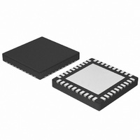
40-VFQFN Exposed Pad
Output Voltage
0.375 V to 1.6 V
Output Current
500 uA
Input Voltage
1.7 V to 24 V
Switching Frequency
0.25 MHz to 6 MHz
Operating Temperature Range
0 C to + 85 C
Mounting Style
SMD/SMT
Duty Cycle (max)
100 %
Isolated/non-isolated
Non Isolated
Lead Free Status / RoHS Status
Lead free / RoHS Compliant
Available stocks
Company
Part Number
Manufacturer
Quantity
Price
Company:

Part Number:
NCP4200MNR2G
Manufacturer:
PHILIPS
Quantity:
124


Write Operations
S—START
P—STOP
R—READ
W—WRITE
A—ACKNOWLEDGE
A—NO ACKNOWLEDGE
The NCP4200 uses the following I
Send Byte
command byte to a slave device as follows:
The following abbreviations are used in the diagrams:
In this operation, the master device sends a single
REPEATED
START BY
SDA
MASTER
SCL
SDA
SCL
START BY
MASTER
SDA
SCL
SDA
SCL
1
1
1
1
START BY
MASTER
SERIAL BUS ADDRESS BYTE
START BY
MASTER
1
1
2
C write protocols.
SERIAL BUS ADDRESS BYTE
1
1
0
0
FRAME 1
1
1
1
0
0
FRAME 1
1
SERIAL BUS ADDRESS BYTE
0
SERIAL BUS ADDRESS BYTE
0
0
0
0
Figure 12. Write Byte
FRAME 1
Figure 11. Send Byte
A1
http://onsemi.com
A1
0
FRAME 1
Figure 13. Read Byte
SDA (CONTINUED)
0
SCL (CONTINUED)
A0
0
A0
A1
NCP4200
ACK. BY
18
A1
R/W
R/W
A0
NCP4200
ACK. BY
A0
R/W
9
9
R/W
NCP4200
ACK. BY
1. The master device asserts a start condition on
2. The master sends the 7−bit slave address followed
3. The addressed slave device asserts ACK on SDA.
4. The master sends a command code.
5. The slave asserts ACK on SDA.
6. The master asserts a stop condition on SDA and
NCP4200
ACK. BY
D7
D7
1
SDA.
by the write bit (low).
the transaction ends.
1
9
D7
1
9
D7
D6
D6
1
D7
D6
1
DATA BYTE FROM NCP4200
D6
D5
D5
D6
D5
D5
D4
COMMAND CODE
D4
FRAME 2
D5
D4
DATA BYTE
FRAME 2
D4
COMMAND CODE
FRAME 3
D3
COMMAND CODE
D3
D4
D3
FRAME 2
D3
FRAME 2
D3
D2
D2
D2
D2
D2
D1
D1
D1
D1
D0
D1
D0
NO ACK. BY
NCP4200
D0
ACK. BY
D0
MASTER
NCP4200
ACK. BY
D0
9
NCP4200
ACK. BY
9
NCP4200
9
9
ACK. BY
9
STOP BY
MASTER
STOP BY
MASTER
STOP BY
MASTER
Related parts for NCP4200MNR2G
Image
Part Number
Description
Manufacturer
Datasheet
Request
R

Part Number:
Description:
Programmable Multi-phase Synchronous Buck Converter With Pmbus
Manufacturer:
ON Semiconductor
Datasheet:
Part Number:
Description:
ON Semiconductor [VOLTAGE REGULATOR]
Manufacturer:
ON Semiconductor
Datasheet:
Part Number:
Description:
357-036-542-201 CARDEDGE 36POS DL .156 BLK LOPRO
Manufacturer:
ON Semiconductor
Datasheet:
Part Number:
Description:
357-036-542-201 CARDEDGE 36POS DL .156 BLK LOPRO
Manufacturer:
ON Semiconductor
Datasheet:
Part Number:
Description:
357-036-542-201 CARDEDGE 36POS DL .156 BLK LOPRO
Manufacturer:
ON Semiconductor
Datasheet:
Part Number:
Description:
357-036-542-201 CARDEDGE 36POS DL .156 BLK LOPRO
Manufacturer:
ON Semiconductor
Datasheet:
Part Number:
Description:
357-036-542-201 CARDEDGE 36POS DL .156 BLK LOPRO
Manufacturer:
ON Semiconductor
Datasheet:
Part Number:
Description:
357-036-542-201 CARDEDGE 36POS DL .156 BLK LOPRO
Manufacturer:
ON Semiconductor
Datasheet:
Part Number:
Description:
357-036-542-201 CARDEDGE 36POS DL .156 BLK LOPRO
Manufacturer:
ON Semiconductor
Datasheet:
Part Number:
Description:
357-036-542-201 CARDEDGE 36POS DL .156 BLK LOPRO
Manufacturer:
ON Semiconductor
Datasheet:
Part Number:
Description:
357-036-542-201 CARDEDGE 36POS DL .156 BLK LOPRO
Manufacturer:
ON Semiconductor
Datasheet:
Part Number:
Description:
357-036-542-201 CARDEDGE 36POS DL .156 BLK LOPRO
Manufacturer:
ON Semiconductor
Datasheet:
Part Number:
Description:
Manufacturer:
ON Semiconductor
Datasheet:
Part Number:
Description:
Manufacturer:
ON Semiconductor
Datasheet: