MAX1531ETJ+ Maxim Integrated Products, MAX1531ETJ+ Datasheet - Page 18

MAX1531ETJ+
Manufacturer Part Number
MAX1531ETJ+
Description
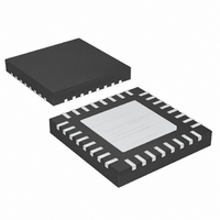
IC PS CTRLR MULTI-OUTPUT 32TQFN
Manufacturer
Maxim Integrated Products
Datasheet
1.MAX1531ETJT.pdf
(33 pages)
Specifications of MAX1531ETJ+
Applications
Five Power Supply Monitor
Voltage - Supply
4.5 V ~ 28 V
Current - Supply
1.7mA
Operating Temperature
-40°C ~ 85°C
Mounting Type
Surface Mount
Package / Case
32-TQFN Exposed Pad
Voltage - Output
1.25 ~ 16.5 V
Number Of Outputs
5
Lead Free Status / RoHS Status
Lead free / RoHS Compliant
Voltage - Input
-
Lead Free Status / Rohs Status
Details
Multiple-Output Power-Supply
Controllers for LCD Monitors
Figure 4. Step-Down Controller Block Diagram
pumps attached to the switching node or extra wind-
ings coupled to the step-down converter inductor. The
negative gain block (MAX1531) can be used in con-
junction with a charge pump or coupled winding to
generate the LCD gate-off voltage or other negative
supplies.
The MAX1530/MAX1531 include step-down controllers
that use a fixed-frequency current-mode PWM control
scheme (Figure 4). An internal transconductance
amplifier establishes an integrated error voltage at the
COMP pin. The heart of the current-mode PWM con-
troller is an open-loop comparator that compares an
integrated voltage-feedback signal with an amplified
current-sense signal plus a slope-compensation ramp.
At each rising edge of the internal clock, the high-side
MOSFET turns on until the PWM comparator trips or the
maximum duty cycle is reached. During this on-time,
current ramps up through the inductor, sourcing cur-
rent to the output and storing energy in a magnetic
field. The current-mode feedback system regulates the
peak inductor current as a function of the output volt-
age error signal. Since the average inductor current is
nearly the same as the peak inductor current (assum-
ing that the inductor value is relatively high to minimize
ripple current), the circuit acts as a switch-mode
transconductance amplifier. That pushes the output LC
filter pole, normally found in a voltage-mode PWM, to a
higher frequency. To preserve loop stability, the slope-
compensation ramp is summed into the main PWM
comparator.
18
DC-DC EN
SS DONE
CLOCK
SLOPE
COMP
______________________________________________________________________________________
V
ILIM
REF
FB
START
SOFT-
0.9VREF
GM
Step-Down Controller
CURRENT
∑
LIMIT
PWM COMP
FAULT COMPARATOR
CURRENT
CURRENT
SENSE
LIMIT
AND
R
S
Q
Q
IN
DH
DL
LX
PGND
FLTM
During the second half of the cycle, the high-side MOS-
FET turns off and the low-side N-channel MOSFET turns
on. Now the inductor releases the stored energy as its
current ramps down, providing current to the output.
The output capacitor stores charge when the inductor
current exceeds the load current and discharges when
the inductor current is lower, smoothing the voltage
across the load. Under overload conditions, when the
inductor current exceeds the selected current limit (see
Current Limit Circuit ), the high-side MOSFET is not
turned on at the rising edge of the clock and the low-
side MOSFET remains on to let the inductor current
ramp down.
Under light-load conditions, the MAX1530/MAX1531
maintain a constant switching frequency to minimize
cross-regulation errors in applications that use a trans-
former. The low-side gate-drive waveform is the comple-
ment of the high-side gate-drive waveform, which
causes the inductor current to reverse under light loads.
The MAX1530/MAX1531s’ current-sense circuit ampli-
fies the current-sense voltage generated by the high-
side MOSFET’s on-resistance. This amplified
current-sense signal and the internal slope compensa-
tion signal are summed together and fed into the PWM
comparator’s inverting input. Place the high-side MOS-
FET near the controller, and connect IN and LX to the
MOSFET using Kelvin-sense connections to guarantee
current-sense accuracy and improve stability.
The MAX1530/MAX1531 include two current-limit cir-
cuits that use the two MOSFETs’ on-resistances as cur-
rent-sensing elements (Figure 4). The high-side
MOSFET’s voltage is used with a fixed 400mV (typ) cur-
rent-limit threshold during the high-side on-times. The
low-side MOSFET’s voltage is used with an adjustable
current-limit threshold during the low-side on-times.
Using both circuits together ensures that the current is
always measured and controlled.
The high-side MOSFET current limit employs a peak
current limit. If the voltage across the high-side MOS-
FET, measured from IN to LX, exceeds the 400mV
threshold during an on-time, the high-side MOSFET
turns off and the low-side MOSFET turns on.
The low-side MOSFET current-limit circuit employs a
“valley” current limit. If the voltage across the low-side
MOSFET, measured from LX to PGND, exceeds the
low-side threshold at the end of a low-side on-time, the
low-side MOSFET remains on and the high-side MOS-
FET stays off for the entire next cycle.
Current-Sense Amplifier
Current-Limit Circuit


