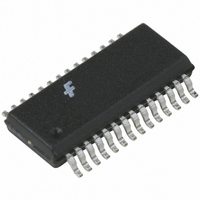
FAN5236QSC Fairchild Semiconductor, FAN5236QSC Datasheet

FAN5236QSC
Specifications of FAN5236QSC
FAN5236QSC_NL
Available stocks
Related parts for FAN5236QSC
FAN5236QSC Summary of contents
Page 1
FAN5236 Dual Mobile-Friendly DDR / Dual-output PWM Controller Features • Highly flexible dual synchronous switching PWM controller includes modes for: – DDR mode with in-phase operation for reduced channel interference – 90˚ phase shifted two-stage DDR Mode for reduced input ...
Page 2
PRODUCT SPECIFICATION Generic Block Diagrams VCC +5 ILIM1 DDR ILIM2/ REF2 VCC +5 ILIM1 DDR +5 PG2/REF 1.25V Figure 2. Complete DDR Memory Power Supply 2 VIN (BATTERY 24V FAN5236 Q1 VOUT1 L = 2.5V OUT1 PWM ...
Page 3
FAN5236 Pin Configurations Pin Definitions Pin Number Pin Name 1 AGND Analog Ground. This is the signal ground reference for the IC. All voltage levels are measured with respect to this pin. 2 LDRV1 Low-Side Drive. The low-side (lower) MOSFET ...
Page 4
PRODUCT SPECIFICATION Pin Definitions (continued) Pin Number Pin Name 14 VIN Input Voltage. Normally connected to battery, providing voltage feed-forward to set the amplitude of the internal oscillator ramp. When using the IC for 2-step conversion from 5V input, connect ...
Page 5
FAN5236 Electrical Specifications Parameter Power Supplies VCC Current VIN Current – Sinking VIN Current – Sourcing VIN Current – Shut-down UVLO Threshold UVLO Hysteresis Oscillator Frequency Ramp Amplitude, pk–pk Ramp Amplitude, pk–pk Ramp Offset Ramp / VIN Gain Ramp / ...
Page 6
PRODUCT SPECIFICATION Electrical Specifications Parameter DDR, EN Inputs Input High Input Low FPWM Inputs FPWM Low FPWM High EN HYST SS OVP DDR RAMP OSC VIN CLK S VSEN EA FPWM/VOUT SS VREF Reference and PGOOD Soft Start REF2 6 ...
Page 7
FAN5236 Typical Applications VIN (BATTERY 24V VCC + ILIM1 11 EN1 8 SS1 PG1 15 DDR +5 13 EN2 21 SS2 17 C3 1.25V@10mA PG2/REF 16 AGND 1 FPWM2 20 ...
Page 8
PRODUCT SPECIFICATION Typical Applications (continued) VIN (BATTERY 24V VCC ILIM1 11 EN1 8 SS1 PG1 15 DDR 13 EN2 21 PG2 16 SS2 17 C3 AGND 1 FPWM2 20 ...
Page 9
FAN5236 Circuit Description Overview The FAN5236 is a multi-mode, dual channel PWM control- ler intended for graphic chipset, SDRAM, DDR DRAM or other low voltage power applications in modern notebook, desktop, and sub-notebook PCs. The IC integrates a control circuitry ...
Page 10
PRODUCT SPECIFICATION CLK VDDQ VTT Figure 8. Noise-susceptible In-Phase operation for DDR2 These problems are nicely solved by delaying the 2 verter’s clock by 90° as shown in Figure 9. In this way, all switching transitions in one converter take ...
Page 11
FAN5236 Hysteretic Mode Conversely, the transition from Hysteretic mode to PWM mode occurs when the SW node is negative for 8 consecutive cycles. A sudden increase in the output current will also cause a change from hysteretic to PWM mode. ...
Page 12
PRODUCT SPECIFICATION Current Processing Section The following discussion refers to Figure 11. The current through R resistor (ISNS) is sampled SENSE shortly after Q2 is turned on. That current is held, and summed with the output of the error amplifier. ...
Page 13
FAN5236 Frequency Loop Compensation Due to the implemented current mode control, the modulator has a single pole response with -1 slope at frequency deter- mined by load --------------------- - where R ...
Page 14
PRODUCT SPECIFICATION PGOOD 1 8 CLK IL 2 VOUT 3 CH1 5.0V CH2 100mV CH2 2.0A Figure 15. Over-Current protection waveforms Over-Voltage / Under-voltage Protection Should the VSNS voltage exceed 120% of VREF (0.9V) due to an upper MOSFET failure, ...
Page 15
FAN5236 Output Capacitor Selection The output capacitor serves two major functions in a switch- ing power supply. Along with the inductor it filters the sequence of pulses produced by the switcher, and it supplies the load transient currents. The output ...
Page 16
PRODUCT SPECIFICATION These losses are given by UPPER SW COND --------------------- - OUT P = -------------- I R COND OUT ...
Page 17
FAN5236 Layout Considerations Switching converters, even during normal operation, produce short pulses of current which could cause substan- tial ringing and be a source of EMI if layout constrains are not observed. There are two sets of critical components in ...
Page 18
PRODUCT SPECIFICATION Mechanical Dimensions 28-Pin QSOP Inches Millimeters Symbol Min. Max. Min. 0.053 1.35 A 0.069 A1 0.004 0.010 0. 0.061 B 0.008 0.012 0.20 C 0.007 0.010 0.18 D 0.386 0.394 9.81 E 0.150 0.157 3.81 ...
Page 19
FAN5236 Mechanical Dimensions 28-Pin TSSOP 9.7 0.1 0.51 TYP 28 PIN # 1 IDENT 1.2 MAX 0.1 C ALL LEAD TIPS – C – 0.65 0.19–0.30 0.13 DIMENSIONS ARE IN MILLIMETERS NOTES: A. Conforms to JEDEC registration MO-153, variation AB, ...
Page 20
... PRODUCT SPECIFICATION Ordering Information Part Number Temperature Range FAN5236QSC -10°C to 85°C FAN5236QSCX -10°C to 85°C FAN5236MTC -10°C to 85°C FAN5236MTCX -10°C to 85°C DISCLAIMER FAIRCHILD SEMICONDUCTOR RESERVES THE RIGHT TO MAKE CHANGES WITHOUT FURTHER NOTICE TO ANY PRODUCTS HEREIN TO IMPROVE RELIABILITY, FUNCTION OR DESIGN. FAIRCHILD DOES NOT ASSUME ANY LIABILITY ARISING OUT OF THE APPLICATION OR USE OF ANY PRODUCT OR CIRCUIT DESCRIBED HEREIN ...


