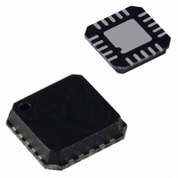
ADM8839ACP-REEL Analog Devices Inc, ADM8839ACP-REEL Datasheet - Page 5

ADM8839ACP-REEL
Manufacturer Part Number
ADM8839ACP-REEL
Description
IC CHARGE PUMP REG TFT 20LFCSP
Manufacturer
Analog Devices Inc
Datasheet
1.ADM8839ACPZ-REEL.pdf
(12 pages)
Specifications of ADM8839ACP-REEL
Rohs Status
RoHS non-compliant
Applications
Converter, TFT, LCD
Voltage - Input
2.7 ~ 4.2 V
Number Of Outputs
3
Voltage - Output
-15V, 5V, 15V
Operating Temperature
-40°C ~ 85°C
Mounting Type
Surface Mount
Package / Case
20-LFCSP
For Use With
ADM8839-EVALZ - BOARD EVALUATION FOR ADM8839
PIN CONFIGURATION AND FUNCTION DESCRIPTIONS
Table 5. Pin Function Descriptions
Pin No.
1
2
3
4
5
6
7
8
9
10
11, 12
13, 14
15, 16
17
18
19, 20
Mnemonic
V
VOUT
LDO_IN
+5VOUT
+5VIN
LDO_ON/OFF
SHDN
V
GND
+15VOUT
C3−, C3+
C2−, C2+
C4−, C4+
−15VOUT
GND
C1−, C1+
CC
CC
Description
Positive Supply Voltage Input. Connect this pin to the 3 V supply with a 2.2 μF decoupling capacitor. Must be
electrically tied together with Pin 8 by a PCB trace.
Voltage Doubler Output. This is derived by doubling the 3 V supply. A 2.2 μF capacitor to ground is required
on this pin.
Voltage Regulator Input. The user can bypass this circuit by using the LDO_ON/OFF pin.
5 V Output. This is derived by doubling and regulating the 3 V supply. A 2.2 μF capacitor to ground is required
on this pin to stabilize the regulator.
5 V Input. This is the input to the voltage tripler and inverter charge pump circuits.
Control Logic Input. 3 V CMOS logic. A logic high selects the internal LDO for regulation of the 5 V voltage
doubler output. A logic low isolates the internal LDO from the rest of the charge pump circuits. This allows the
use of an external LDO to regulate the 5 V voltage doubler output. The output of this LDO is then fed back into
the voltage tripler and inverter circuits of the ADM8839.
Digital Input. 3 V CMOS logic. Active low shutdown control. This shuts down the timing generator and enables
the discharge circuit to dissipate the charge on the voltage outputs, thus driving them to 0 V.
Connect this pin to V
Connect this pin to GND. Must be electrically tied with Pin 18 by a PCB trace.
15 V Output. This is derived by tripling the 5 V regulated output. A 0.22 μF capacitor is required on this pin.
External Capacitor C3 is connected between these pins. A 0.22 μF capacitor is recommended.
External Capacitor C2 is connected between these pins. A 0.22 μF capacitor is recommended.
External Capacitor C4 is connected between these pins. A 0.22 μF capacitor is recommended.
−15 V Output. This is derived by tripling and inverting the 5 V regulated output. A 0.22 μF capacitor is required
on this pin.
Device Ground. Must be electrically tied with Pin 9 by a PCB trace.
External Capacitor C1 is connected between these pins. A 2.2 μF capacitor is recommended.
CC
. Must be electrically tied with Pin 1 by a PCB trace.
+5VOUT 4
LDO_IN 3
VOUT 2
+5VIN 5
V
CC
Figure 2. Pin Configuration
1
Rev. C | Page 5 of 12
ADM8839
TOP VIEW
PIN 1
INDICATOR
15 C4–
14 C2+
13 C2–
12 C3+
11 C3–
ADM8839


