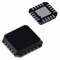
ADM8839ACP-REEL Analog Devices Inc, ADM8839ACP-REEL Datasheet - Page 8

ADM8839ACP-REEL
Manufacturer Part Number
ADM8839ACP-REEL
Description
IC CHARGE PUMP REG TFT 20LFCSP
Manufacturer
Analog Devices Inc
Datasheet
1.ADM8839ACPZ-REEL.pdf
(12 pages)
Specifications of ADM8839ACP-REEL
Rohs Status
RoHS non-compliant
Applications
Converter, TFT, LCD
Voltage - Input
2.7 ~ 4.2 V
Number Of Outputs
3
Voltage - Output
-15V, 5V, 15V
Operating Temperature
-40°C ~ 85°C
Mounting Type
Surface Mount
Package / Case
20-LFCSP
For Use With
ADM8839-EVALZ - BOARD EVALUATION FOR ADM8839
ADM8839
THEORY OF OPERATION
POWER SEQUENCING
For the TFT panel to power up correctly, the gate drive supplies
must be sequenced such that the −15 V supply is up before the
+15 V supply. The ADM8839 controls this sequence. When the
device is turned on (a logic high on SHDN ), the ADM8839
allows the −15 V output to ramp immediately but holds off the
+15 V output. It continues to do this until the negative output
has reached −3 V. At this point, the positive output is enabled
and allowed to ramp to +15 V. This sequence is highlighted in
Figure 14.
TRANSIENT RESPONSE
The ADM8839 features extremely fast transient response,
making it very suitable for fast image updates on TFT LCD
panels. This means that even under changing load conditions,
there is still very effective regulation of the 5 V output. Figure 11
and Figure 12 show how the 5 V output responds when a
maximum load is dynamically connected and disconnected.
Note that the output settles within 5 μs to less than 1% of the
output level.
V
SHDN
+5V
+15V
–15V
CC
90%
10%
t
FM15V
10%
t
DELAY
10%
90%
Figure 14. Power Sequence
90%
t
–3V
R5V
t
R15V
t
t
t
F5V
F15V
RM15V
Rev. C | Page 8 of 12
BOOSTING THE CURRENT DRIVE OF THE ±15 V
SUPPLY
The ADM8839 ±15 V output can deliver 150 μA of current in
the typical configuration, as shown in Figure 15. It is also
possible to draw 100 μA from the +15 V output and 200 μA
from the −15 V output, or vice versa. It is possible to draw a
maximum of only 300 μA combined from the +15 V and the
−15 V outputs at any time (see Figure 16). In this configuration,
+5VOUT (Pin 4) is connected to +5VIN (Pin 5), as shown in
the functional block diagram (see Figure 1).
LDO_ON/OFF
SHDN
15.1
15.0
14.9
14.8
14.7
14.6
14.5
14.4
14.3
14.2
14.1
Figure 16. +15 V/−15 V Output Voltage vs. Load Current,
0
ADM8839
OSCILLATOR
GENERATOR
SHUTDOWN
CONTROL
CONTROL
TIMING
LOGIC
Figure 15. Typical Configuration
50
Typical Configuration
DISCHARGE
V
CC
GND
I
LOAD
–15V AT 25°C
100
C5, 2.2µF
REGULATOR
VOLTAGE
TRIPLER
(µA)
DOUBLE
VOLTAGE
TRIPLE
INVERTER
DOUBLER
VOLTAGE
VOLTAGE
LDO
+15V AT 25°C
150
C1+
C1–
VOUT
LDO_IN
+5VOUT
+5VIN
C2+
C2–
C3+
C3–
+15VOUT
C4+
C4–
–15VOUT
C1, 2.2µF
C2, 0.22µF
C3, 0.22µF
C4, 0.22µF
C6, 2.2µF
C7, 2.2µF
C8, 0.22µF
C9, 0.22µF
200
+5V
+15V
–15V


