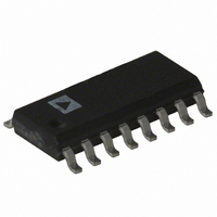
ADP3157JR-REEL Analog Devices Inc, ADP3157JR-REEL Datasheet - Page 10

ADP3157JR-REEL
Manufacturer Part Number
ADP3157JR-REEL
Description
IC CNTRL SYNC PENTIUM III 16SOIC
Manufacturer
Analog Devices Inc
Datasheet
1.ADP3157JR.pdf
(12 pages)
Specifications of ADP3157JR-REEL
Rohs Status
RoHS non-compliant
Applications
Controller, Intel Pentium® III
Voltage - Input
12V
Number Of Outputs
1
Voltage - Output
1.3 ~ 3.5 V
Operating Temperature
0°C ~ 70°C
Mounting Type
Surface Mount
Package / Case
16-SOIC (3.9mm Width)
ADP3157
To correctly implement active voltage positioning, the low fre-
quency output impedance (i.e., the output resistance) of the
converter should be made equal to the maximum ESR of the
output capacitor array. This can be achieved by having a single
pole roll-off of the voltage gain of the g
the pole frequency coincides with the ESR zero of the output
capacitor. A gain with single pole roll-off requires that the g
amplifier output pin be terminated by the parallel combination
of a resistor and capacitor. The required resistor value can be
calculated from the equation:
where
and where the quantities 16.4 k and 275 k are characteristics
of the ADP3157 and the value of the current sense resistor, R
has already been determined as above.
Although a single termination resistor equal to R
the proper voltage positioning gain, the dc biasing of that resis-
tor would determine how the regulation band is centered (i.e.,
offset). Note that sometimes the specified regulation band is
asymmetrical with respect to the nominal VID voltage. With the
ADP3157, the offset is already considered as part of the design
procedure—no special provision is required. To accomplish the
dc biasing, it is simplest to use two resistors to terminate the g
amplifier output, with the lower resistor tied to ground and the
upper resistor to the 12 V supply of the IC. The values of these
resistors can be calculated using:
where V
ommended 12 V), and V
amplifier to produce the desired offset at the output. V
calculated using Equation 2 below, where V
from the nominal VID-programmed value to the center of the
specified regulation window for the output voltage. (Note this
may be either positive or negative.) For clarification, that offset
is given by:
where V
allowed for regulation.
and
DIV
HI
and V
is the resistor divider supply voltage (e.g., the rec-
Rt
LO
V
V
R
TOTAL
OUT OS
OS
LOWER
are the respective upper and lower limits
R
C
(
R
UPPER
OS
Rt
)
275
275
16 4 .
TOTAL
R
is the offset voltage required on the
1
2
C
R
(
V
k
k
C
k
R
HI
V
C
HI
–
V
V
R
DIV
Rt
Rt
–
V
0 8
V
CS
LO
.
V
DIV
m
V
OS
TOTAL
TOTAL
LO
)–
OS
V
error amplifier, where
–
I
V
VID
OMAX
OUT(OS)
OS
V
OUT OS
C
would yield
(
is the offset
)
OS
1 36
Rt
.
is
TOTAL
m
k
CS
m
,
–10–
– .
1 7
Finally, the compensating capacitance is determined from the
equality of the pole frequency of the error amplifier gain and the
zero frequency of the impedance of the output capacitor:
Trade-Offs Between DC Load Regulation and AC Load
Regulation
Casual observation of the circuit operation—e.g., with a voltmeter
—would make it appear that the dc load regulation appears
to be rather poor compared to a conventional regulator. This
would be especially noticeable under very light or very heavy
loads where the voltage is “positioned” near one of the extremes
of the regulation window rather than near the nominal center
value. It must be noted and understood that this low gain char-
acteristic (i.e., loose dc load regulation) is inherently required to
allow improved transient containment (i.e., to achieve tighter ac
load regulation). That is, the dc load regulation is intentionally
sacrificed (but kept within specification) in order to minimize
the number of capacitors required to contain the load transients
produced by the CPU.
LAYOUT AND COMPONENT PLACEMENT GUIDELINES
The following guidelines are recommended for optimal perfor-
mance of a switching regulator in a PC system:
General Recommendations
1.
2.
3.
V
For best results, a four-layer (minimum) PCB is recom-
mended. This should allow the needed versatility for con-
trol circuitry interconnections with optimal placement, a
signal ground plane, power planes for both power ground
and the input power (e.g., 5 V), and wide interconnection
traces in the rest of the power delivery current paths. Each
square unit of 1 ounce copper trace has a resistance of
Whenever high currents must be routed between PCB
layers, vias should be used liberally to create several parallel
current paths so that the resistance and inductance intro-
duced by these current paths is minimized and the via cur-
rent rating is not exceeded.
The power and ground planes should overlap each other as
little as possible. It is generally easiest (although not neces-
sary) to have the power and signal ground planes on the
same PCB layer. The planes should be connected nearest
to the first input capacitor where the input ground current
flows from the converter back to the power source (e.g.,
5 V).
~0.53 mW at room temperature.
Rt
275
TOTAL
k
6
R I
CS OMAX
C
COMP
C
Rt
O
TOTAL
ESR
REV. A
(2)


