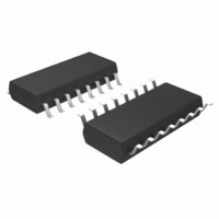
MIC9131BM Micrel Inc, MIC9131BM Datasheet - Page 14

MIC9131BM
Manufacturer Part Number
MIC9131BM
Description
IC CTRLR DC-DC PWM HV HS 16-SOIC
Manufacturer
Micrel Inc
Datasheet
1.MIC9131YM.pdf
(19 pages)
Specifications of MIC9131BM
Applications
Controller, Telecom
Voltage - Input
9 ~ 18 V
Number Of Outputs
1
Voltage - Output
4.7 ~ 5 V
Operating Temperature
-40°C ~ 125°C
Mounting Type
Surface Mount
Package / Case
16-SOIC (3.9mm Width)
Lead Free Status / RoHS Status
Contains lead / RoHS non-compliant
Available stocks
Company
Part Number
Manufacturer
Quantity
Price
MIC9131
The gate impedance of a MOSFET is capacitive and the
power required to drive the gate is proportional to the charge
required to turn on the MOSFET, the peak gate voltage and
the switching frequency. Assuming the total gate charge for
turn on and turn off is equal, the power used to switch the
MOSFET on and off is:
where: Q
The power required to drive the MOSFET is dissipated in the
drive circuitry of the MIC9131. This power must not cause
the die temperature to exceed the maximum rated junction
temperature of 125°C.
MOSFET Driver IC’s are used when the drive requirement for
the MOSFETs is greater than the capability of the MIC9131
gate drive output. While the peak current of the MIC9131
gate drive is typically 1.2A at V
will sink or source between 1.2A and 12A of peak current.
The higher peak current allows faster rise and fall times for
larger MOSFETs.
The drive requirements for selecting a MOSFET driver are
determined using the following equation:
where: Q
For example, if a MOSFET is chosen with a Q
it is desired to have a 50nS gate to source risetime/falltime,
the peak current requirement of the MOSFET driver is:
A driver such as the MIC4424 will meet this requirement.
For more information on choosing a MOSFET driver, see
the Micrel application note AN-24, “Designing with Low Side
MOSFET Drivers.”
M9999-080206
V
usually equal to V
f
the MOSFET at a specified I
information is usually given in the MOSFET
specification sheet.
t is the gate voltage transition time (risetime or fall
time)
I
MOSFET driver IC.
I
P
I
PK
S
PK
PK
DRIVE
GS
G
G
is the output switching frequency
=
= ×
is the peak current requirement of the
is the total gate charge at V
is the total gate charge required to turn on
is the gate to source voltage of the MOSFET
2
2 60
Gate Drive
×
50
=
Output
Q
Q
ns
t
G
nC
G
GND
×
V
=
GS
2 4 .
Figure 10
C1
CC
×
A
f
S
1:N
T1
IN
R1
D2
D1
=12V, a gate driver ICs
D
, V
GS
G
and V
R2
G
of 60nC and
DS
. This
14
Current Sense Circuit
The current sense input of the MIC9131 has three unique
features, which are advantageous in a high speed, high ef-
ficiency power supply.
The current limit threshold of the ISNS pin was set at 0.82V,
allowing the use of a smaller current sense resistor. A stable,
bandgap derived 40µA current is sourced from the ISNS pin.
A voltage drop across a series resistor placed between the
pin and the current sense resistor level increases the current
sense signal at the ISNS pin. This allows the use of a smaller
current sense resistor if the full 0.82V peak to peak current
signal is not required. Decreasing the value of the current
sense resistor decreases the power dissipation in the resistor,
which improves the efficiency of the power supply.
The delay between the input of the overcurrent comparator
and the output gate drive is nominally 50ns. This very fast
response time allows the MIC9131 to operate at higher fre-
quencies and still have adequate overcurrent protection.
The operation of the current sense input is as follows. The
sensed current in the power supply is converted to a volt-
age by a resistor or current sense transformer. Referring to
Figure 1, this voltage is compared to the output of the error
amplifier, which sets the duty cycle of the gate drive output.
The current signal is also connected to an Imax comparator.
Comparing the current sense signal to the reference voltage
sets a maximum current limit. If the maximum amplitude of the
current sense signal exceeds the reference, the comparator
terminates the gate drive output pulse. It aslo discharges the
soft start capacitor when the CPWR pin is high.
Leading Edge Current Spike
The current signal in a power circuit will often have a leading
edge spike caused by leakage inductance, parasitic induc-
tance and capacitance, diode reverse recovery effects and
snubbers. These spikes can cause premature termination of
the switching cycle if they are not eliminated.
A resistor may be added in series between the current sense
resistor and the Isns input. The input and board trace ca-
pacitance of the ISNS pin (pin 14) is approximately 25pF. A
1k resistor is a good choice, since it attenuates most of the
ripple without distorting the current sense waveform. It has
a minimal effect on level, offsetting the current sense signal
by only 40mV.
A typical rule of thumb is the bandwidth of the RC filter
should be at least 6 times the switching frequency. This
avoids distorting the current sense waveform and adding
excessive delays in the current loop that will interfering with
overcurrent protection. For a 100kHz switcher, the maximum
1. The overcurrent threshold is nominally 0.82V instead
2. The current sense pin sources a nominal 40µA of
3. The delay from the current sense input to the output
of the typical 1.0V found in most switching control
ICs.
cur rent out of the pin. This is used to raise the current
limit threshold of the pin, which allows a smaller
current sense resistor to be used. This improves the
efficiency of the power supply, especially in lower
current applications.
is typically 50ns.
August 2006
Micrel, Inc.


