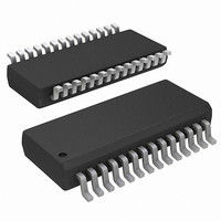
ISL6227CA Intersil, ISL6227CA Datasheet - Page 11

ISL6227CA
Manufacturer Part Number
ISL6227CA
Description
IC CONTROLLER DDR, DDR2 28QSOP
Manufacturer
Intersil
Datasheet
1.ISL6227CAZ.pdf
(27 pages)
Specifications of ISL6227CA
Applications
Controller, DDR, DDR2
Voltage - Input
5 ~ 28 V
Number Of Outputs
2
Voltage - Output
0.9 ~ 5.5 V
Operating Temperature
-10°C ~ 100°C
Mounting Type
Surface Mount
Package / Case
28-QSOP
Lead Free Status / RoHS Status
Contains lead / RoHS non-compliant
Available stocks
Company
Part Number
Manufacturer
Quantity
Price
Part Number:
ISL6227CA
Manufacturer:
INTERSIL
Quantity:
20 000
Company:
Part Number:
ISL6227CAZ
Manufacturer:
HARRIS
Quantity:
8
Company:
Part Number:
ISL6227CAZ
Manufacturer:
Intersil
Quantity:
1 645
Part Number:
ISL6227CAZ
Manufacturer:
INTERSIL
Quantity:
20 000
Company:
Part Number:
ISL6227CAZ-T
Manufacturer:
Intersil
Quantity:
2 500
Part Number:
ISL6227CAZ-T
Manufacturer:
INTERSIL
Quantity:
20 000
PG2/REF
This pin has a double function, depending on the mode of
operation.
When the chip is used as a dual channel PWM controller
(DDR = 0), the pin provides an open drain PGOOD2 function
for the second channel the same way as PG1. The pin is
pulled low when the second channel output is out of
-11% to +15% of the set value.
In DDR mode (DDR = 1), this pin is the output of the buffer
amplifier that takes VDDQ/2 voltage applied to OCSET2 pin
from the resister divider. It can source a typical 10mA
current.
OCSET2
In a dual channel application with DDR = 0, a resistor from
this pin to ground sets the overcurrent threshold for the
second channel controller. Its voltage is the buffered internal
0.9V reference.
In the DDR application with DDR = 1, this pin connects to the
center point of a resistor divider tracking the VDDQ/2. This
voltage is then buffered by an amplifier voltage follower and
sent to the PG2/REF pin. It sets the reference voltage of
Channel 2 for its regulation.
VCC
This pin powers the controller.
11
ISL6227
Typical Application
Figures 31 and 32 show the application circuits of a dual
channel DC/DC converter for a notebook PC.
The power supply in Figure 31 provides +2.5V and +1.8V
voltages for memory and the graphics interface chipset from
a +5.0VDC to a 28VDC battery voltage.
Figure 32 illustrates the application circuit for a DDR memory
power solution. The power supply shown in Figure 32
generates +2.5V VDDQ voltage from a battery. The +1.25V
VTT termination voltage tracks VDDQ/2 and is derived from
+2.5V VDDQ. To complete the DDR memory power
requirements, the +1.25V reference voltage is provided
through the PG2 pin.
May 4, 2009
FN9094.7


