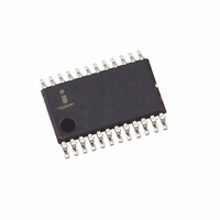
EL5825IRZ Intersil, EL5825IRZ Datasheet - Page 8

EL5825IRZ
Manufacturer Part Number
EL5825IRZ
Description
IC TFT-LCD VREF GEN 24-TSSOP
Manufacturer
Intersil
Datasheet
1.EL5825IR.pdf
(12 pages)
Specifications of EL5825IRZ
Applications
Converter, TFT, LCD
Voltage - Input
4.5 ~ 16.5 V
Number Of Outputs
8
Voltage - Output
0.5 ~ 14.95 V
Operating Temperature
-40°C ~ 85°C
Mounting Type
Surface Mount
Package / Case
24-TSSOP
Lead Free Status / RoHS Status
Lead free / RoHS Compliant
Internal Refresh Clock Oscillator
The EL5825 requires an internal clock or external clock to
refresh its outputs. The outputs are refreshed at the falling
OSC clock edges. The output refreshed switches open at
the rising edges of the OSC clock. The driving load shouldn’t
be changed at the rising edges of the OSC clock. Otherwise,
it will generate a voltage error at the outputs. This clock may
be input or output via the clock pin labeled OSC. The internal
clock is provided by an internal oscillator running at
approximately 25kHz and can be output to the OSC pin. In a
multiple chip system, if the driving loads are stable, one chip
may be programmed to use the internal oscillator; then the
OSC pin will output the clock from the internal oscillator.
Subsequent chips may have the OSC pin connected to this
clock source. In these chips, the program will set them to
external OSC Mode by setting bit 14 to 1. See the control
bits logic table and serial programming example for details.
For transient load application, the external clock Mode
should be used to ensure all functions are synchronized
together. The positive edge of the external clock to the OSC
pin should be timed to avoid the transient load effect. The
Application Drawing on page 10 shows the LCD H rate
signal used, here the positive clock edge is timed to avoid
the transient load of the column driver circuits.
After power on, the chip will start with the internal oscillator
mode. At this time, the OSC pin will be in a high impedance
Block Diagram
SERIAL DATA INPUT
SERIAL CLOCK
8
ENABLE
REGISTERS
CHANNEL
EIGHT
EL5825
CONTROL IF
SOURCES
VOLTAGE
condition to prevent contention. After programming the
oscillator with bit 14, the pin will be set to the appropriate
mode.
Transfer Function
The transfer function is:
where data is the decimal value of the 10-bit data binary
input code.
The output voltages from the EL5825 will be derived from
the reference voltages present at the V
pins. The impedance between those two pins is about 32kΩ.
Care should be taken that the system design holds these
two reference voltages within the limits of the power rails of
the EL5825. GND < V
V
In some LCD applications that require more than 8 channels,
the system can be designed such that one EL5825 will
provide the Gamma correction voltages that are more
positive than the V
provide the Gamma correction voltage more negative than
the V
shows a system connected in this way.
V
REFH
OUT IDEAL )
COM
(
.
potential. The Application Drawing on page 10
OSCILLATOR INPUT/OUTPUT3
=
V
REFL
COM
REFH
+
REFERENCE HIGH
OUTA
OUTB
OUTC
OUTD
OUTE
OUTF
OUTG
OUTH
REFERENCE LOW
CAP
SERIAL DATA OUTPUT
potential. The second EL5825 can
data
------------ -
1024
≤ V
×
(
S
V
REFH
and GND ≤ V
REFL
- V
REFL
and V
REFL
)
June 24, 2005
REFH
≤
FN7005.4


