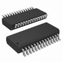
ISL6225CA Intersil, ISL6225CA Datasheet - Page 11

ISL6225CA
Manufacturer Part Number
ISL6225CA
Description
IC CTRLR DDR DRAM, SDRAM 28QSOP
Manufacturer
Intersil
Datasheet
1.ISL6225CAZ.pdf
(19 pages)
Specifications of ISL6225CA
Applications
Controller, DDR DRAM, SDRAM
Voltage - Input
5 ~ 24 V
Number Of Outputs
2
Voltage - Output
0.9 ~ 5.5 V
Operating Temperature
-10°C ~ 85°C
Mounting Type
Surface Mount
Package / Case
28-QSOP
Lead Free Status / RoHS Status
Contains lead / RoHS non-compliant
Available stocks
Company
Part Number
Manufacturer
Quantity
Price
Company:
Part Number:
ISL6225CA
Manufacturer:
INTERSIL
Quantity:
36
Company:
Part Number:
ISL6225CA
Manufacturer:
Intersil
Quantity:
467
Part Number:
ISL6225CA
Manufacturer:
ISL
Quantity:
20 000
Company:
Part Number:
ISL6225CA-T
Manufacturer:
INTERSIL
Quantity:
980
Part Number:
ISL6225CA-T
Manufacturer:
INTERSIL
Quantity:
20 000
Company:
Part Number:
ISL6225CAZ
Manufacturer:
Intersil
Quantity:
1 889
Part Number:
ISL6225CAZ
Manufacturer:
INTERSIL
Quantity:
20 000
Company:
Part Number:
ISL6225CAZ-T
Manufacturer:
INTERSIL
Quantity:
1 608
Part Number:
ISL6225CAZ-T
Manufacturer:
INTERSIL
Quantity:
20 000
The zero frequency, the amplifier high-frequency gain, and
the modulator gain are chosen to satisfy most typical
applications. The crossover frequency will appear at the
point where the modulator attenuation equals the amplifier
high frequency gain. The only task that the system designer
has to complete is to specify the output filter capacitors to
position the load main pole somewhere within one decade
lower than the amplifier zero frequency. With this type of
compensation plenty of phase margin is easily achieved due
to zero-pole pair phase ‘boost’. Conditional stability may
occur only when the main load pole is positioned too much
to the left side on the frequency axis due to excessive output
filter capacitance. In this case, the ESR zero placed within
10kHz...50kHz range gives some additional phase ‘boost’.
Some phase boost can also be achieved by connecting
capacitor C
divider that sets the output voltage value, as shown in
Figure 4.
Gate Control Logic
The gate control logic translates generated PWM signals
into gate drive signals providing necessary amplification,
level shift, and shoot-trough protection. Also, it bears some
functions that help to optimize the IC performance over a
wide range of the operational conditions. As MOSFET
switching time can very dramatically from type to type and
with the input voltage, the gate control logic provides
adaptive dead time by monitoring real gate waveforms of
both the upper and the lower MOSFETs.
Dual-Step Conversion
The ISL6225 dual channel controller can be used either in
power systems with a single-stage power conversion when
the battery power is converted into the desired output
voltage in one step, or in the systems where some
intermediate voltages are initially established. The choice of
the approach may be dictated by the overall system design
criteria or simply to be a matter of voltages available to the
system designer, like in the case of PCI card applications.
When the power input voltage is a regulated 5V or 3.3V
system bus, the feed-forward ramp may become too
shallow, which creates the possibility of duty-factor jitter
especially in a noisy environment. The noise susceptibility
when operating from low level regulated power sources can
be improved by connecting the VIN pin to ground. The feed-
forward ramp generator will be internally reconnected from
the VIN pin to the V
doubled. Application circuits for dual-step power conversion
are presented in Figures 11 through 15.
z
in parallel with the upper resistor R1 of the
CC
pin and the ramp slew rate will be
11
ISL6225
Protections
The converter output is monitored and protected against
extreme overload, short circuit, Overvoltage, and
Undervoltage conditions.
A sustained overload on the output sets the PGOOD low and
latches-off the whole chip. The controller operation can be
restored by cycling the VCC voltage or an enable (EN) pin.
Overcurrent Protection
Both PWM controllers use the lower MOSFET’s
on-resistance {r
against shorted outputs. The sensed current from the ISEN
pin is compared with a current set by a resistor connected
from the OCSET pin to ground.
Where, I
R
the I
If the lower MOSFET current exceeds the overcurrent
threshold, a pulse skipping circuit is activated. The upper
MOSFET will not be turned on as long as the sensed
current is higher then the threshold value. This limits the
current supplied by the DC voltage source. This condition
keeps on for eight clock cycles after the overcurrent
comparator was tripped for the first time. If after these first
eight clock cycles the current exceeds the overcurrent
threshold again in a time interval of another eight clock
cycles, the overcurrent protection latches and disables the
chip. If the overcurrent condition goes away during the first
eight clock cycles, normal operation is restored and the
overcurrent circuit resets itself sixteen clock cycles after the
overcurrent threshold was exceeded the first time, Figure 8.
R OCSET
3
CS
1
2
FIGURE 8. OVERCURRENT PROTECTION WAVEFORMS
SEN
CH1 5.0V
is the value of the current sense resistor connected to
CH3 1.0AΩ
IL
OC
pin.
=
is a desired overcurrent protection threshold and
9.6V
--------------------------------------------------------- -
I OC R
DS(ON)
PGOOD
•
VOUT
(
•
R CS
CH2 100mV
DS ON
} to monitor the current for protection
+
(
100Ω
8 CLK
)
)
SHUTDOWN
December 28, 2004
M 10.0µs
FN9049.7


