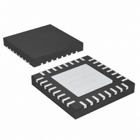
MAX8744AETJ+ Maxim Integrated Products, MAX8744AETJ+ Datasheet - Page 14

MAX8744AETJ+
Manufacturer Part Number
MAX8744AETJ+
Description
IC CNTRLR PWR SUP QUAD 32TQFN
Manufacturer
Maxim Integrated Products
Datasheet
1.MAX8744AETJ.pdf
(36 pages)
Specifications of MAX8744AETJ+
Applications
Controller, Notebook Computers
Voltage - Input
6 ~ 26 V
Number Of Outputs
4
Voltage - Output
3.3V, 5V, 1 ~ 26 V
Operating Temperature
0°C ~ 85°C
Mounting Type
Surface Mount
Package / Case
32-TQFN Exposed Pad
Lead Free Status / RoHS Status
Lead free / RoHS Compliant
High-Efficiency, Quad-Output, Main Power-
Supply Controllers for Notebook Computers
14
______________________________________________________________________________________
PIN
15
16
17
18
19
20
21
22
23
24
25
26
27
28
29
30
31
PGOODA
PGOOD3
NAME
PGND
LDO5
CSH3
CSL3
BST5
BST3
DH5
DH3
FBA
LX5
DL5
DL3
LX3
FB3
IN
Boost Flying Capacitor Connection for the 5V SMPS. The MAX8744A/MAX8745A include an internal
boost switch connected between LDO5 and BST5. Connect to an external capacitor as shown in
Figure 1.
High-Side Gate-Driver Output for the 5V SMPS. DH5 swings from LX5 to BST5.
Inductor Connection for the 5V SMPS. Connect LX5 to the switched side of the inductor. LX5 serves
as the lower supply rail for the DH5 high-side gate driver.
Low-Side Gate-Driver Output for the 5V SMPS. DL5 swings from PGND to LDO5.
Power Ground
5V Internal Linear-Regulator Output. Bypass with 4.7µF minimum (1µF/25mA). Provides at least
100mA for the DL_ low-side gate drivers, the DH_ high-side drivers through the BST switches, the
PWM controller, logic, reference, and external loads. If CSL5 is greater than 4.5V and soft-start is
complete, the linear regulator shuts down, and LDO5 connects to CSL5 through a 1Ω switch rated for
loads up to 200mA.
Input of the Startup Circuitry and the LDO5 Internal 5V Linear Regulator. Bypass to PGND with a
0.22µF or greater ceramic capacitor close to the IC.
Open-Drain, Power-Good Output for the Auxiliary LDO. PGOODA is pulled low if FBA drops more
than 10% (typ) below the normal regulation point, and when the auxiliary LDO is shut down. PGOODA
becomes high impedance when FBA is in regulation.
Low-Side Gate-Driver Output for the 3.3V SMPS. DL3 swings from PGND to LDO5.
Inductor Connection for the 3.3V SMPS. Connect LX3 to the switched side of the inductor. LX3 serves
as the lower supply rail for the DH3 high-side gate driver.
High-Side Gate-Driver Output for the 3.3V SMPS. DH3 swings from LX3 to BST3.
Boost Flying Capacitor Connection for the 3.3V SMPS. The MAX8744A/MAX8745A include an internal
boost switch connected between LDO5 and BST3. Connect to an external capacitor as shown in
Figure 1.
Open-Drain, Power-Good Output for the 3.3V SMPS. PGOOD3 is pulled low if CSL3 drops more than
10% (typ) below the normal regulation point. PGOOD3 is held low during soft-start and shutdown.
PGOOD3 becomes high impedance when CSL3 is in regulation.
Output Sense and Negative Current Sense for the 3.3V SMPS. When using the internal preset 3.3V
feedback divider (FB3 = LDO5), the controller uses CSL3 to sense the output voltage. Connect to the
negative terminal of the current-sense element.
Positive Current-Sense Input for the 3.3V SMPS. Connect to the positive terminal of the current-sense
element. Figure 7 describes two different current-sensing options—using accurate sense resistors or
lossless inductor DCR sensing.
Feedback Input for the 3.3V SMPS. Connect to LDO5 for fixed 3.3V output. In adjustable mode, FB3
regulates to 2V.
Auxiliary LDO Feedback Input. Connect a resistive voltage-divider from OUTA to analog ground to
adjust the auxiliary linear-regulator output voltage. FBA regulates at 1V.
FUNCTION
Pin Description (continued)


