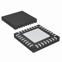
MAX8744AETJ+ Maxim Integrated Products, MAX8744AETJ+ Datasheet - Page 22

MAX8744AETJ+
Manufacturer Part Number
MAX8744AETJ+
Description
IC CNTRLR PWR SUP QUAD 32TQFN
Manufacturer
Maxim Integrated Products
Datasheet
1.MAX8744AETJ.pdf
(36 pages)
Specifications of MAX8744AETJ+
Applications
Controller, Notebook Computers
Voltage - Input
6 ~ 26 V
Number Of Outputs
4
Voltage - Output
3.3V, 5V, 1 ~ 26 V
Operating Temperature
0°C ~ 85°C
Mounting Type
Surface Mount
Package / Case
32-TQFN Exposed Pad
Lead Free Status / RoHS Status
Lead free / RoHS Compliant
High-Efficiency, Quad-Output, Main Power-
Supply Controllers for Notebook Computers
The switching waveforms may appear noisy and asyn-
chronous when light loading causes pulse-skipping
operation, but this is a normal operating condition that
results in high light-load efficiency. Trade-offs in PFM
noise vs. light-load efficiency are made by varying the
inductor value. Generally, low inductor values produce
a broader efficiency vs. load curve, while higher values
result in higher full-load efficiency (assuming that the
coil resistance remains fixed) and less output-voltage
ripple. Penalties for using higher inductor values
include larger physical size and degraded load-tran-
sient response (especially at low input-voltage levels).
DC output accuracy specifications in the Electrical
Characteristics table refer to the error comparator’s
threshold. When the inductor continuously conducts,
the MAX8744A/MAX8745A regulate the peak of the out-
put ripple, so the actual DC output voltage is lower than
the slope-compensated trip level by 50% of the output
ripple voltage. For PWM operation (continuous conduc-
tion), the output voltage is accurately defined by the fol-
lowing equation:
where V
equals 1.1%, and V
(V
Output Capacitor Selection section).
In discontinuous conduction (I
MAX8744A/MAX8745A regulate the valley of the output
ripple, so the output voltage has a DC regulation level
higher than the error-comparator threshold. For PFM
operation (discontinuous conduction), the output volt-
age is approximately defined by the following equation:
where V
maximum switching frequency set by the internal oscil-
lator, f
the idle mode inductor current when pulse skipping.
Connect FB3 and FB5 to LDO5 to enable the fixed
SMPS output voltages (3.3V and 5V, respectively), set
by a preset, internal resistive voltage-divider connected
between the output (CSL_) and analog ground.
Connect a resistive voltage-divider at FB_ between the
output (CSL_) and GND to adjust the respective output
voltage between 2V and 5.5V (Figure 5). Choose R
(resistance from FB to GND) to be approximately 10kΩ
22
V
RIPPLE
OUT PWM
______________________________________________________________________________________
SW
(
NOM
V
NOM
OUT PFM
is the actual switching frequency, and I
= ESR x ΔI
)
=
is the nominal output voltage, f
(
is the nominal output voltage, A
V
NOM
)
=
RIPPLE
⎛
⎜
⎝
V
1
INDUCTOR
NOM
−
A
SLOPE RIPPLE
+
is the output ripple voltage
1
2
V
⎛
⎜
⎝
OUT
IN
f
V
, as described in the
OSC
f
SW
Output Voltage
< I
⎞
⎟
⎠
I
IDLE
LOAD(SKIP)
⎞
⎟ −
⎠
ESR
⎛
⎜
⎝
V
OSC
RIPPLE
2
SLOPE
IDLE
is the
), the
FBLO
⎞
⎟
⎠
is
and solve for R
using the equation:
where V
When adjusting both output voltages, set the 3.3V
SMPS lower than the 5V SMPS. LDO5 connects to the
5V output (CSL5) through an internal switch only when
CSL5 is above the LDO5 bootstrap threshold (4.5V)
and the soft-start sequence for the CSL5 side has com-
pleted. Bootstrapping works most effectively when the
fixed output voltages are used. Once LDO5 is boot-
strapped from CSL5, the internal 5V linear regulator
turns off. This reduces the internal power dissipation
and improves efficiency at higher input voltages.
The current-limit circuit uses differential current-sense
inputs (CSH_ and CSL_) to limit the peak inductor cur-
rent. If the magnitude of the current-sense signal
exceeds the current-limit threshold, the PWM controller
turns off the high-side MOSFET (Figure 3). The actual
maximum load current is less than the peak current-
limit threshold by an amount equal to half of the induc-
tor ripple current. Therefore, the maximum load
capability is a function of the current-sense resistance,
inductor value, switching frequency, and duty cycle
(V
Figure 5. Dual Mode Feedback Decoder
OUT
LDO5
/V
OUT
FB
FB_
IN
AMPLIFIER
).
TO ERROR
= 2V nominal.
9R
R
FBHI
FBHI
Current-Limit Protection (ILIM)
R
=
(resistance from the output to FB)
R
FBLO
FIXED OUTPUT
ADJUSTABLE
⎛
⎜
⎝
FB = LDO5
OUTPUT
V
V
OUT
FB
_
_
−
1
⎞
⎟
⎠


