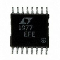
LT1977EFE#PBF Linear Technology, LT1977EFE#PBF Datasheet - Page 19

LT1977EFE#PBF
Manufacturer Part Number
LT1977EFE#PBF
Description
IC REG SW 1.5A HV STP DN 16TSSOP
Manufacturer
Linear Technology
Type
Step-Down (Buck)r
Datasheet
1.LT1977EFEPBF.pdf
(24 pages)
Specifications of LT1977EFE#PBF
Internal Switch(s)
Yes
Synchronous Rectifier
No
Number Of Outputs
1
Voltage - Output
1.2 ~ 54 V
Current - Output
1.5A
Frequency - Switching
500kHz
Voltage - Input
3.3 ~ 60 V
Operating Temperature
-40°C ~ 125°C
Mounting Type
Surface Mount
Package / Case
16-TSSOP Exposed Pad, 16-eTSSOP, 16-HTSSOP
Primary Input Voltage
60V
No. Of Outputs
1
Output Voltage
54V
Output Current
3.5A
No. Of Pins
16
Operating Temperature Range
-40°C To +125°C
Msl
MSL 1 - Unlimited
Rohs Compliant
Yes
Dc To Dc Converter Type
Step Down
Pin Count
16
Input Voltage
60V
Switching Freq
575KHz
Package Type
TSSOP EP
Output Type
Adjustable
Switching Regulator
Yes
Mounting
Surface Mount
Input Voltage (min)
2.4V
Operating Temp Range
-40C to 125C
Operating Temperature Classification
Automotive
Lead Free Status / RoHS Status
Lead free / RoHS Compliant
Power - Output
-
Lead Free Status / Rohs Status
Compliant
Available stocks
Company
Part Number
Manufacturer
Quantity
Price
APPLICATIO S I FOR ATIO
the user to generate a delayed signal after the power good
threshold is exceeded.
Referring to Figure 2, the PGFB pin is the positive input to
a comparator whose negative input is set at V
PGFB is taken above V
the C
the PGFB pin drops below V
100k TO V
500mV/DIV
500mV/DIV
T
2V/DIV
V
pin starting the delay period. When the voltage on
V
SHDN
OUT
V
PG
CT
IN
PG at 80% V
V
OUT
Figure 9. Power Good
LT1977
LT1977
U
PGFB
PGFB
PGFB
Disconnect at 80% V
TIME (10ms/DIV)
with 100ms Delay
V
V
PG
PG
FB
C
FB
C
IN
IN
T
T
U
, current (I
OUT
PGFB
with 100ms Delay
0.27µF
0.27µF
200k
W
the C
CSS
200k
153k
12k
100k
153k
12k
100k
) is sourced into
T
OUT
1977 F09
pin is rapidly
PGFB
C
C
Figure 10. Power Good Circuits
OUT
OUT
U
V
OUT
. When
= 3.3V
V
OUT
= 3.3V
discharged resetting the delay period. The PGFB voltage is
typically generated by a resistive divider from the regu-
lated output or input supply.
The capacitor on the C
delay time between the PGFB pin exceeding its threshold
(V
When the PGFB pin rises above V
(I
voltage on the external capacitor reaches an internal clamp
(V
resultant PG delay time is given by t = C
the voltage on the PGFB pin drops below its V
be discharged rapidly and PG will be active low with a
200µA sink capability. If the SHDN pin is taken below its
threshold during normal operation, the C
discharged and PG inactive, resulting in a non Power Good
cycle when SHDN is taken above its threshold. Figure 9
shows the power good operation with PGFB connected to
FB and the capacitance on C
V
CT
PG at V
OUT
PGFB
CT
) from the C
), the PG pin becomes a high impedance node. The
LT1977
LT1977
Disconnect 3.3V Logic Signal
) and the PG pin set to a high impedance state.
PGFB
PGFB
IN
with 100µs Delay
V
V
PG
PG
FB
C
FB
C
IN
IN
T
T
> 4V with 100ms Delay
T
511k
200k
pin into the external capacitor. When the
0.27µF
270pF
200k
200k
165k
100k
866k
100k
1977 F10
T
pin determines the amount of
T
C
= 0.1µF. The PGOOD pin has
OUT
C
V
OUT
OUT
PGFB
V
= 3.3V
OUT
current is sourced
= 12V
CT
• (V
LT1977
T
PGFB
pin will be
CT
)/(I
, C
19
CT
CT
1977fa
). If
will


