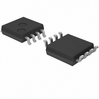
BD9306AFVM-TR Rohm Semiconductor, BD9306AFVM-TR Datasheet

BD9306AFVM-TR
Specifications of BD9306AFVM-TR
Available stocks
Related parts for BD9306AFVM-TR
BD9306AFVM-TR Summary of contents
Page 1
... BD9305AFVM Description BD9305AFVM / BD9306AFVM are 1-channel DC/DC converter controllers. Step-down DC/DC converter can be configured by BD9305AFVM, and Step-up DC/DC converter can be configured by BD9306AFVM. In addition, the master slave function, which is that the synchronization is possible at the time of multi-connection, is mounted. Features 1) 1ch PWM Control DC/DC Converter Controller 2) Input Voltage Range:4.2 to 18V 3) Feed Back Voltage:1.25± ...
Page 2
... COMP Sink Current COMP Source Current 【Gate Drive Block】 ON Resistance Gate Drive Voltage L Gate Drive Voltage H MAX Duty (BD9305AFVM) MAX Duty (BD9306AFVM) 【Control Block】 ON Voltage OFF Voltage ENB Sink Current 【Soft Start Block】 Soft Start Time 【Timer Latch Protection Circuit】 ...
Page 3
... BD9306AFVM, BD9305AFVM Electrical Characteristics (Unless otherwise specified,V 1 0.5 Ta=25 ℃ Ta=85 ℃ 0 Ta=40 ℃ -0 INPUT VOLTAGE:VCC[V] Fig.1 Standby Circuit Current 1000 800 600 400 200 VOLTAGE:VGD[V] Fig.4 GD Sink Current 0 -20 -40 -60 -80 -100 0 0.5 1 1.5 2 2.5 COMP VOLTAGE:VCOMP[V] Fig.7 COMP Source Current www.rohm.com © ...
Page 4
... BD9306AFVM, BD9305AFVM Electrical Characteristics (Unless otherwise specified,Ta=25℃) 250 Ta=85 ℃ 200 Ta=25 ℃ 150 100 50 Ta=-40 ℃ 0 0.0 2.5 5.0 7.5 10.0 12.5 ENB VOLTAGE:VENB[V] Fig.10 ENB Input Current -40 - AMBIENT TEMPERATURE[ ℃ ] Fig.13 Temperature vs MAX Duty (BD9306AFVM) Δ V=380mV Io=500mA VCC=12V Vo=16V Fig ...
Page 5
... BD9306AFVM, BD9305AFVM Block Diagram Fig19. Pin Assignment Diagram & Block Diagram (Above:BD9305AFVM / Below:BD9306AFVM) Pin Assignment and Pin Function Pin No Pin Name GND 7 COMP 8 www.rohm.com © 2009 ROHM Co., Ltd. All rights reserved. FB COMP 7 8 Err 1.25V OSC COMP 8 7 Err 1.25V OSC ...
Page 6
... OSC 1 RT 20kΩ Fig.20 Block Diagram / Application Circuit (BD9305AFVM Err 1.25V OSC 1 RT 20Ω Fig.21 Block Diagram / Application Circuit (BD9306AFVM) www.rohm.com © 2009 ROHM Co., Ltd. All rights reserved. 10000pF 5.1kΩ GND Vcc COMP Soft Start Vref ...
Page 7
... CT. ・PWM The Duty is determined by comparing the output of Error amplifier and the angular wave of Oscillator. The switching Duty of BD9306AFVM is limited by the maximum duty ratio that is determined by the internal part, and will not 100%. ・DRV The gate of the power FET that is connected to the outside is driven by the switching Duty determined by PWM. ...
Page 8
... We recommend 10kΩ~330kΩ as the setting range resistance below 10kΩ is set, a drop in voltage efficiency will be caused resistance more than 330kΩ is set, the offset voltage becomes large because of the internal error amplifier’s input bias current of 0.05µA(Typ). Please set the maximum setting voltage of BD9306AFVM (step up) in such a way that Duty : (Vo - Vcc less than 70%. ...
Page 9
... Furthermore, each parameter has a deviation of 30%~40%, so please design in such a way that you have left a sufficient margin for deviation in your design. (8)Setting of Power FET If step-down DC/DC is configured by BD9305AFVM, Pch FET is necessary; if step-up DC/DC is configured by BD9306AFVM, Nch FET is necessary. Please pay attention to the following conditions when you choose. <step-down DC/DC> Maximum inductor current ...
Page 10
... BD9306AFVM, BD9305AFVM (9) Phase compensation Phase Setting Method The following conditions are required in order to ensure the stability of the negative feedback circuit. Phase lag should be 150° or lower during gain 1 (0 dB) (phase margin of 30° or higher). Because DC/DC converter applications are sampled using the switching frequency, the overall GBW should be set to 1/10 the switching frequency or lower. The target application characteristics can be summarized as follows: ...
Page 11
... Slave Function> The master slave function, which is that the synchronous switching is possible by using these IC of BD9305AFVM / BD9306AFVM through their multi-connection, is mounted. The following drawing shows an example of connection circuit in which BD9305AFVM is connected on the master side and BD9306AFVM is connected on the slave side. VCC CTL1 ...
Page 12
... BD9306AFVM, BD9305AFVM I/O Equivalent Circuit Diagram Fig.32 1.RT VCC VREF 2.CT VCC VREF 3.ENB www.rohm.com © 2009 ROHM Co., Ltd. All rights reserved. 4.GD VCC A VCC(BD9305AFVM) A: GND(BD9306AFVM) 7.COMP VCC VREF 8.FB VCC VREF Fig. 32 12/14 Technical Note 2009.05 - Rev.A ...
Page 13
... BD9306AFVM, BD9305AFVM Notes for use 1) Absolute maximum ratings Use of the IC in excess of absolute maximum ratings such as the applied voltage or operating temperature range may result in IC damage. Assumptions should not be made regarding the state of the IC (short mode or open mode) when such damage is suffered. A physical safety measure such as a fuse should be implemented when use of the special mode where the absolute maximum ratings may be exceeded is anticipated ...
Page 14
... BD9306AFVM, BD9305AFVM Ordering part number Part No. Part No. 9306A 9305A MSOP8 2.9±0.1 (MAX 3.25 include BURR) + 6° 4° −4° 1PIN MARK 0.145 0.475 S +0.05 0.22 –0.04 0.08 S 0.65 www.rohm.com © 2009 ROHM Co., Ltd. All rights reserved Package FVM: MSOP8 <Tape and Reel information> ...
Page 15
No copying or reproduction of this document, in part or in whole, is permitted without the consent of ROHM Co.,Ltd. The content specified herein is subject to change for improvement without notice. The content specified herein is for the purpose ...


